| **System** | ||
| 1. | Dimension | 101 x 119 x 17.5 mm |
| 2. | Case | ABS, black |
| 3. | Working environment | Indoor |
| 4. | Working temperature | -30 | +70 |
| 5. | Recommended operating conditions | 5 – 60°C and 20 – 80%RH; |
| 6. | Configuration | USB – configuration terminal via com port |
| 7. | Firmware upgrade | USB – mass storage device |
| **Electrical specifications** | ||
| 8. | Inputs | 16-bit resolution, Input resistance: ~1 MOhm Input capacitance: ~170 pF Input Ranges: ±10 V (amplitude); Nominal values: - Current input: - 225 mV (rms); - Voltage input: - 1.876 V (rms); Overvoltage protection of all inputs up to ±20 V (amplitude) |
| **Power** | ||
| 9. | Power Supply | 9 V to 33 V |
| 10. | Current consumption | 40 mA @ 12 VDC, 20 mA @ 24 VDC |
It is highly advised to exit the main screen before disconnecting the device
If the terminal window is closed accidentally, a user can connect the terminal program again, and press any key on a keyboard to show the main menu again. #### Configuration terminal menu| Menu Name | Submenu | Values | Default Values | |
| \[S\] | Process parameters | \[1\] Set rated primary voltage \[2\] Set rated primary current | 1–65000 V 1–65000 A | 1 V 1 A |
| \[P\] | Communication protocol | \[1\] IEC103 \[2\] Modbus RTU | - - | Modbus RTU |
| \[1\] | Link or device Address | Set link or device address | 1–254 | 1 |
| \[2\] | Baud rate, Parity and Stop bits | \[1\] Set 8 Data bits + 1 Stop bit \[2\] Set 8 Data bits + 2 Stop bit \[3\] Configure baud rate \[4\] Configure Parity | - - 100–256000 None/ Odd / Even / Mark/ Space | 1 Stop bit 9600 Even |
| \[3\] | RS485 Terminating Resistor | \[1\] Enable \[2\] Disable | - - | Disabled |
| \[4\] | Configure sensors | \[1\] – magnitude factor of voltage sensor 1 \[2\] – magnitude factor of voltage sensor 2 \[3\] – magnitude factor of voltage sensor 3 \[4\] – magnitude factor of voltage sensor 4 \[5\] – current sensor nominal value | 100–3000 100–3000 100–3000 100–3000 100–3000 mV | 1000 1000 1000 1000 225 mV |
| \[5\] | Select measurand set and scale factor\* \*(this menu is visible only when the IEC103 protocol is activated) | \[1\] Measurand set 1 \[2\] Measurand set 2 \[3\] Measurand set 3 \[4\] Measurand set 4 \[5\] Scale factor 1.2 \[6\] Scale factor 2.4 \[7\] Function type | - - - - - - 1–255 | Measurand set 4 Scale factor 1.2 253 |
| \[6\] | Set nominal system frequency | \[1\] – 50 Hz \[2\] – 60 Hz | - - | 50 Hz |
| \[7\] | Set Default Settings | \[1\] - confirm \[0\] - cancel | - - | - |
| \[8\] | Firmware Upgrade | \[1\] - confirm \[0\] - cancel | - - | - |
| \[9\] | Diagnostics | Raw input values | - | - |
| \[0\] | Exit | Exit and disconnect | - | - |
| **Set Nr.** | **TYPE** | **FUN\*** | **INF** | **Qty** **of data** | **Information elements (measurands)** |
| 1 | 9 | 253 | 148 | 9 | I1, I2, I3, U1, U2, U3, P, Q, f |
| 2 | 9 | 253 | 149 | 23 | I1, I2, I3, I4, U1, U2, U3, U4, P1, P2, P3, Q1, Q2, Q3, S1, S2, S3, PF1, PF2, PF3, U12ph, U23ph, U13ph |
| 3 | 9 | 253 | 150 | 60 | I1, I2, I3, IN, U1, U2, U3, UN, P1, P2, P3, Q1, Q2, Q3, S1, S2, S3, PF1, PF2, PF3, U12, U23, U13, f, THDU1, THDU2, THDU3, THDI1, THDI2, THDI3, I1\_H2, I1\_H3, I1\_H5, I1\_H7, I1\_H9, I2\_H2, I2\_H3, I2\_H5, I2\_H7, I2\_H9, I3\_H2, I3\_H3, I3\_H5, I3\_H7, I3\_H9, U1\_H2, U1\_H3, U1\_H5, U1\_H7, U1\_H9, U2\_H2, U2\_H3, U2\_H5, U2\_H7, U2\_H9, U3\_H2, U3\_H3, U3\_H5, U3\_H7, U3\_H9 |
| 4 | 9 | 253 | 151 | 54 | I1, I2, I3, IN, U12, U23, U13, UN, S, P, Q, PF, THDU1, THDU2, THDU3, THDI1, THDI2, THDI3, I1\_H3, I1\_H5, I1\_H7, I1\_H9, I2\_H3, I2\_H5, I2\_H7, I2\_H9, I3\_H3, I3\_H5, I3\_H7, I3\_H9, U1\_H3, U1\_H5, U1\_H7, U1\_H9, U2\_H3, U2\_H5, U2\_H7, U2\_H9, U3\_H3, U3\_H5, U3\_H7, U3\_H9, P1, P2, P3, Q1, Q2, Q3, U1ph, U2ph, U3ph, U1, U2, U3 |
| No. | Designation | Measured quantity |
| 1 | I1 | Phase L1 current with standard scaling (1.2 or 2.4) |
| 2 | I2 | Phase L2 current with standard scaling (1.2 or 2.4) |
| 3 | I3 | Phase L3 current with standard scaling (1.2 or 2.4) |
| 4 | I4 | IN channel current with standard scaling (1.2 or 2.4) |
| 5 | U1 | Phase L1 voltage with standard scaling (1.2 or 2.4) |
| 6 | U2 | Phase L2 voltage with standard scaling (1.2 or 2.4) |
| 7 | U3 | Phase L3 voltage with standard scaling (1.2 or 2.4) |
| 8 | U4 | UN channel voltage with standard scaling (1.2 or 2.4) |
| 9 | P1 | Phase L1 real power with standard scaling (1.2 or 2.4) |
| 10 | P2 | Phase L2 real power with standard scaling (1.2 or 2.4) |
| 11 | P3 | Phase L3 real power with standard scaling (1.2 or 2.4) |
| 12 | P | Total 3 phase real power (P1+P2+P3) with standard scaling (1.2 or 2.4) divided by 3 |
| 13 | Q1 | Phase L1 reactive power with standard scaling (1.2 or 2.4) |
| 14 | Q2 | Phase L2 reactive power with standard scaling (1.2 or 2.4) |
| 15 | Q3 | Phase L3 reactive power with standard scaling (1.2 or 2.4) |
| 16 | Q | Total 3 phase reactive power (Q1+Q2+Q3) with standard scaling (1.2 or 2.4) divided by 3 |
| 17 | S1 | Phase L1 apparent power with standard scaling (1.2 or 2.4) |
| 18 | S2 | Phase L2 apparent power with standard scaling (1.2 or 2.4) |
| 19 | S3 | Phase L3 apparent power with standard scaling (1.2 or 2.4) |
| 20 | S | Total 3 phase apparent power (S1+S2+S3) with standard scaling (1.2 or 2.4) divided by 3 |
| 21 | PF1 | Phase L1 power factor with standard scaling (1.2 or 2.4) |
| 22 | PF2 | Phase L2 power factor with standard scaling (1.2 or 2.4) |
| 23 | PF3 | Phase L3 power factor with standard scaling (1.2 or 2.4) |
| 24 | PF | Total 3-phase power factor with standard scaling (1.2 or 2.4) |
| 25 | U12ph | Phase angle between U1 and U2 without scaling in 0.1deg |
| 26 | U23ph | Phase angle between U2 and U3 without scaling in 0.1deg |
| 27 | U13ph | Phase angle between U1 and U3 without scaling in 0.1deg |
| 28 | f | Phase L1 voltage frequency with fixed scaling 50 |
| 29 | IN | Calculated neutral current with standard scaling (1.2 or 2.4) |
| 30 | UN | Calculated neutral voltage with standard scaling (1.2 or 2.4) |
| 31 | U12 | Calculated phase-to-phase voltage with standard scaling (1.2 or 2.4) divided by SQRT(3) |
| 32 | U23 | Calculated phase-to-phase voltage with standard scaling (1.2 or 2.4) divided by SQRT(3) |
| 33 | U13 | Calculated phase-to-phase voltage with standard scaling (1.2 or 2.4) divided by SQRT(3) |
| 34 | THDU1 | Total harmonic distortions of U1 voltage in 0.1% |
| 35 | THDU2 | Total harmonic distortions of U2 voltage in 0.1% |
| 36 | THDU3 | Total harmonic distortions of U3 voltage in 0.1% |
| 37 | THDI1 | Total harmonic distortions of I1 current in 0.1% |
| 38 | THDI2 | Total harmonic distortions of I2 current in 0.1% |
| 39 | THDI3 | Total harmonic distortions of I3 current in 0.1% |
| 40 | I1\_H2 | 2nd harmonic level of I1 current in 0.1% |
| 41 | I1\_H3 | 3rd harmonic level of I1 current in 0.1% |
| 42 | I1\_H5 | 5th harmonic level of I1 current in 0.1% |
| 43 | I1\_H7 | 7th harmonic level of I1 current in 0.1% |
| 44 | I1\_H9 | 9th harmonic level of I1 current in 0.1% |
| 45 | I2\_H2 | 2nd harmonic level of I2 current in 0.1% |
| 46 | I2\_H3 | 3rd harmonic level of I2 current in 0.1% |
| 47 | I2\_H5 | 5th harmonic level of I2 current in 0.1% |
| 48 | I2\_H7 | 7th harmonic level of I2 current in 0.1% |
| 48 | I2\_H9 | 9th harmonic level of I2 current in 0.1% |
| 49 | I3\_H2 | 2nd harmonic level of I3 current in 0.1% |
| 50 | I3\_H3 | 3rd harmonic level of I3 current in 0.1% |
| 51 | I3\_H5 | 5th harmonic level of I3 current in 0.1% |
| 52 | I3\_H7 | 7th harmonic level of I3 current in 0.1% |
| 53 | I3\_H9 | 9th harmonic level of I3 current in 0.1% |
| 54 | U1\_H2 | 2nd harmonic level of U1 voltage in 0.1% |
| 55 | U1\_H3 | 3rd harmonic level of U1 voltage in 0.1% |
| 56 | U1\_H5 | 5th harmonic level of U1 voltage in 0.1% |
| 57 | U1\_H7 | 7th harmonic level of U1 voltage in 0.1% |
| 58 | U1\_H9 | 9th harmonic level of U1 voltage in 0.1% |
| 59 | U2\_H2 | 2nd harmonic level of U2 voltage in 0.1% |
| 60 | U2\_H3 | 3rd harmonic level of U2 voltage in 0.1% |
| 61 | U2\_H5 | 5th harmonic level of U2 voltage in 0.1% |
| 62 | U2\_H7 | 7th harmonic level of U2 voltage in 0.1% |
| 63 | U2\_H9 | 9th harmonic level of U2 voltage in 0.1% |
| 64 | U3\_H2 | 2nd harmonic level of U3 voltage in 0.1% |
| 65 | U3\_H3 | 3rd harmonic level of U3 voltage in 0.1% |
| 66 | U3\_H5 | 5th harmonic level of U3 voltage in 0.1% |
| 67 | U3\_H7 | 7th harmonic level of U3 voltage in 0.1% |
| 68 | U3\_H9 | 9th harmonic level of U3 voltage in 0.1% |
| 69 | U1ph | Phase angle of U1 without scaling in 0.1deg |
| 70 | U2ph | Phase angle of U2 without scaling in 0.1deg |
| 71 | U3ph | Phase angle of U3 without scaling in 0.1deg |
| **Address** **(Dec)** | **Designation** | **Parameter** | **Multiplier** | **Read/** **Write** | **Unit** |
| 0 | I1 | Phase L1 current | Data \* 100 | R | % |
| 1 | I2 | Phase L2 current | Data \* 100 | R | % |
| 2 | I3 | Phase L3 current | Data \* 100 | R | % |
| 3 | I0 | Calculated neutral current | Data \* 100 | R | % |
| 4 | U12 | Calculated phase to phase voltage L1 – L2 | Data \* 100 | R | % |
| 5 | U23 | Calculated phase to phase voltage L2 – L3 | Data \* 100 | R | % |
| 6 | U13 | Calculated phase to phase voltage L1 – L3 | Data \* 100 | R | % |
| 7 | U0 | Calculated zero sequence voltage | Data \* 100 | R | % |
| 8 | S | Total 3 phase apparent power (S1+S2+S3) | Data \* 100 | R | % |
| 9 | P | Total 3 phase active power (P1+P2+P3) | Data \* 100 | R | % |
| 10 | Q | Total 3 phase reactive power (Q1+Q2+Q3) | Data \* 100 | R | % |
| 11 | PF | Total 3 phase power factor | Data \* 100 | R | % |
| 12 | THDU1 | Total harmonic distortions of U1 voltage | Data \* 100 | R | % |
| 13 | THDU2 | Total harmonic distortions of U2 voltage | Data \* 100 | R | % |
| 14 | THDU3 | Total harmonic distortions of U3 voltage | Data \* 100 | R | % |
| 15 | THDI1 | Total harmonic distortions of I1 current | Data \* 100 | R | % |
| 16 | THDI2 | Total harmonic distortions of I2 current | Data \* 100 | R | % |
| 17 | THDI3 | Total harmonic distortions of I3 current | Data \* 100 | R | % |
| 18 | I1\_H3 | 3nd harmonic level of I1 current | Data \* 100 | R | % |
| 19 | I1\_H5 | 5nd harmonic level of I1 current | Data \* 100 | R | % |
| 20 | I1\_H7 | 7nd harmonic level of I1 current | Data \* 100 | R | % |
| 21 | I1\_H9 | 9nd harmonic level of I1 current | Data \* 100 | R | % |
| 22 | I2\_H3 | 3nd harmonic level of I2 current | Data \* 100 | R | % |
| 23 | I2\_H5 | 5nd harmonic level of I2 current | Data \* 100 | R | % |
| 24 | I2\_H7 | 7nd harmonic level of I2 current | Data \* 100 | R | % |
| 25 | I2\_H9 | 9nd harmonic level of I2 current | Data \* 100 | R | % |
| 26 | I3\_H3 | 3nd harmonic level of I3 current | Data \* 100 | R | % |
| 27 | I3\_H5 | 5nd harmonic level of I3 current | Data \* 100 | R | % |
| 28 | I3\_H7 | 7nd harmonic level of I3 current | Data \* 100 | R | % |
| 29 | I3\_H9 | 9nd harmonic level of I3 current | Data \* 100 | R | % |
| 30 | U1\_H3 | 3nd harmonic level of U1 voltage | Data \* 100 | R | % |
| 31 | U1\_H5 | 5nd harmonic level of U1 voltage | Data \* 100 | R | % |
| 32 | U1\_H7 | 7nd harmonic level of U1 voltage | Data \* 100 | R | % |
| 33 | U1\_H9 | 9nd harmonic level of U1 voltage | Data \* 100 | R | % |
| 34 | U2\_H3 | 3nd harmonic level of U2 voltage | Data \* 100 | R | % |
| 35 | U2\_H5 | 5nd harmonic level of U2 voltage | Data \* 100 | R | % |
| 36 | U2\_H7 | 7nd harmonic level of U2 voltage | Data \* 100 | R | % |
| 37 | U2\_H9 | 9nd harmonic level of U2 voltage | Data \* 100 | R | % |
| 38 | U3\_H3 | 3nd harmonic level of U3 voltage | Data \* 100 | R | % |
| 39 | U3\_H5 | 5nd harmonic level of U3 voltage | Data \* 100 | R | % |
| 40 | U3\_H7 | 7nd harmonic level of U3 voltage | Data \* 100 | R | % |
| 41 | U3\_H9 | 9nd harmonic level of U3 voltage | Data \* 100 | R | % |
| 42 | P1 | Phase L1 active power | Data \* 100 | R | % |
| 43 | P2 | Phase L2 active power | Data \* 100 | R | % |
| 44 | P3 | Phase L3 active power | Data \* 100 | R | % |
| 45 | Q1 | Phase L1 reactive power | Data \* 100 | R | % |
| 46 | Q2 | Phase L2 reactive power | Data \* 100 | R | % |
| 47 | Q3 | Phase L3 reactive power | Data \* 100 | R | % |
| 48 | U1ph | Phase angle of U1 voltage | Data \* 100 | R | deg |
| 49 | U2ph | Phase angle of U2 voltage | Data \* 100 | R | deg |
| 50 | U3ph | Phase angle of U3 voltage | Data \* 100 | R | deg |
| 51 | U1 | Phase L1 voltage | Data \* 100 | R | % |
| 52 | U2 | Phase L2 voltage | Data \* 100 | R | % |
| 53 | U3 | Phase L3 voltage | Data \* 100 | R | % |
| 54 | F | Frequency of phase L1 voltage | Data \* 100 | R | Hz |
| 55 | I4 | Input I4 current | Data \* 100 | R | % |
| 56 | U4 | Input U4 voltage | Data \* 100 | R | % |
| **Address** **(Dec)** | **Designation** | **Parameter** | **Multiplier** | **Read/** **Write** | **Unit** |
| 75 | PC | Primary current value | Data | R/W | A |
| 76 | PV | Primary voltage value | Data | R/W | V |
| 77 | VS1 | Amplitude correction factor U1 | Data | R/W | - |
| 78 | VS2 | Amplitude correction factor U2 | Data | R/W | - |
| 79 | VS3 | Amplitude correction factor U3 | Data | R/W | - |
| 80 | VS4 | Amplitude correction factor U4 | Data | R/W | - |
| 81 | CS1 | Current sensor nominal value | Data | R/W | mV |
| **Address** **(Dec)** | **Designation** | **Parameter** | **Multiplier** | **Read/** **Write** | **Unit** |
| 100 | I1 | Phase L1 current | R | A | |
| 102 | I2 | Phase L2 current | R | A | |
| 104 | I3 | Phase L3 current | R | A | |
| 106 | I0 | Calculated neutral current | R | A | |
| 108 | U12 | Calculated phase to phase voltage L1 – L2 | R | V | |
| 110 | U23 | Calculated phase to phase voltage L2 – L3 | R | V | |
| 112 | U13 | Calculated phase to phase voltage L1 – L3 | R | V | |
| 114 | U1 | Phase L1 voltage | R | V | |
| 116 | U2 | Phase L2 voltage | R | V | |
| 118 | U3 | Phase L3 voltage | R | V | |
| 120 | U0 | Calculated zero sequence voltage | R | V | |
| 122 | U1ph | Phase angle of U1 voltage | R | deg | |
| 124 | U2ph | Phase angle of U2 voltage | R | deg | |
| 126 | U3ph | Phase angle of U3 voltage | R | deg | |
| 128 | S | Total 3 phase apparent power | R | kVA | |
| 130 | P | Total 3 phase active power | R | kW | |
| 132 | Q | Total 3 phase reactive power | R | kVAr | |
| 134 | PF | Total 3 phase power factor | R | - | |
| 136 | S1 | Phase L1 apparent power | R | kVA | |
| 138 | S2 | Phase L2 apparent power | R | kVA | |
| 140 | S3 | Phase L3 apparent power | R | kVA | |
| 142 | P1 | Phase L1 active power | R | kW | |
| 144 | P2 | Phase L2 active power | R | kW | |
| 146 | P3 | Phase L3 active power | R | kW | |
| 148 | Q1 | Phase L1 reactive power | R | kVAr | |
| 150 | Q2 | Phase L2 reactive power | R | kVAr | |
| 152 | Q3 | Phase L3 reactive power | R | kVAr | |
| 154 | PF1 | Phase L1 power factor | R | - | |
| 156 | PF2 | Phase L2 power factor | R | - | |
| 158 | PF3 | Phase L3 power factor | R | - | |
| 160 | F | Frequency of phase L1 voltage | Hz | ||
| 162 | THDU1 | Total harmonic distortions of U1 voltage | R | % | |
| 164 | THDU2 | Total harmonic distortions of U2 voltage | R | % | |
| 166 | THDU3 | Total harmonic distortions of U3 voltage | R | % | |
| 168 | THDI1 | Total harmonic distortions of I1 current | R | % | |
| 170 | THDI2 | Total harmonic distortions of I2 current | R | % | |
| 172 | THDI3 | Total harmonic distortions of I3 current | R | % | |
| 174 | I1\_H3 | 3nd harmonic level of I1 current | R | % | |
| 176 | I1\_H5 | 5nd harmonic level of I1 current | R | % | |
| 178 | I1\_H7 | 7nd harmonic level of I1 current | R | % | |
| 180 | I1\_H9 | 9nd harmonic level of I1 current | R | % | |
| 182 | I2\_H3 | 3nd harmonic level of I2 current | R | % | |
| 184 | I2\_H5 | 5nd harmonic level of I2 current | R | % | |
| 186 | I2\_H7 | 7nd harmonic level of I2 current | R | % | |
| 188 | I2\_H9 | 9nd harmonic level of I2 current | R | % | |
| 190 | I3\_H3 | 3nd harmonic level of I3 current | R | % | |
| 192 | I3\_H5 | 5nd harmonic level of I3 current | R | % | |
| 194 | I3\_H7 | 7nd harmonic level of I3 current | R | % | |
| 196 | I3\_H9 | 9nd harmonic level of I3 current | R | % | |
| 198 | U1\_H3 | 3nd harmonic level of U1 voltage | R | % | |
| 200 | U1\_H5 | 5nd harmonic level of U1 voltage | R | % | |
| 202 | U1\_H7 | 7nd harmonic level of U1 voltage | R | % | |
| 204 | U1\_H9 | 9nd harmonic level of U1 voltage | R | % | |
| 206 | U2\_H3 | 3nd harmonic level of U2 voltage | R | % | |
| 208 | U2\_H5 | 5nd harmonic level of U2 voltage | R | % | |
| 210 | U2\_H7 | 7nd harmonic level of U2 voltage | R | % | |
| 212 | U2\_H9 | 9nd harmonic level of U2 voltage | R | % | |
| 214 | U3\_H3 | 3nd harmonic level of U3 voltage | R | % | |
| 216 | U3\_H5 | 5nd harmonic level of U3 voltage | R | % | |
| 218 | U3\_H7 | 7nd harmonic level of U3 voltage | R | % | |
| 220 | U3\_H9 | 9nd harmonic level of U3 voltage | R | % | |
| 222 | I4 | Input I4 current | R | A | |
| 224 | U4 | Input U4 voltage | R | V |
It is recommended to close the terminal window after entering firmware upgrade mode
The device should then reconnect as a mass storage device (Fig. 10.1). [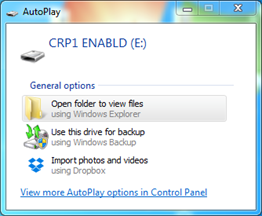](https://wiki.elseta.com/uploads/images/gallery/2021-06/image-1623935180203.png)Fig. 10.1. Reconnecting as a mass storage device Delete the existing file “firmware.bin” and simply upload a new firmware file by dragging and dropping as in Fig. 10.2. [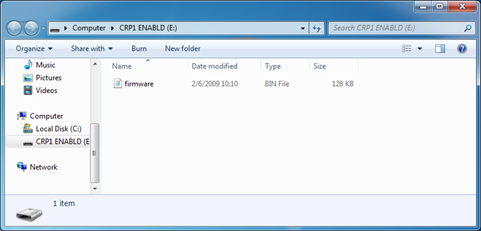](https://wiki.elseta.com/uploads/images/gallery/2021-06/image-1623935213196.png)Fig. 10.2 Mass storage device for firmware upload Reconnect the device and check the firmware version. It should have changed.