IOMOD 4Cs4Vs
IOMod 4Cs4Vs is a compact-sized stand-alone power meter used for measuring analog AC input signals from low power current and voltage sensors. It measures three phases of AC voltages and currents with additional input for neutral/residual voltage and current. Measured and calculated values transmitted to the host system via industry standard IEC 60870-5-103 and Modbus RTU communication protocols.
Firmware version 1
IOMOD 4Cs4Vs User Manual
Introduction
IOMod 4Cs4Vs is a compact-sized stand-alone power meter for measuring analog AC input signals from low-power current and voltage sensors. It measures three phases of AC voltages and currents with additional inputs for neutral/residual voltage and current. The measured and calculated values are transmitted to the host system via communication protocol IEC 60870-5-103 or Modbus RTU.
Features
- 4 AC current sensor inputs according to IEC 60044-8 (nominal value 225mV)
- 4 AC voltage sensor inputs according to IEC 60044-7 (nominal value 3.25/ √3 V)
- Communication protocols : IEC 60870-5-103 or Modbus RTU
- 32 samples per cycle
- FFT-based calculation with harmonic information
- RS485 interface with a switchable terminating resistor
- Status and data transmission (Rx and Tx) indication.
- Configurable over USB
- Drag-and-Drop firmware upgrade over USB
- A small-sized case with a removable front panel
- DIN rail mount
- Operating temperature: from -30 to +70°C
- Power Requirements: 12-24 VDC
Common configuration information
- Nominal system frequency. In order to get correct three-phase system measurements, a user must select nominal system frequency – either 50 Hz or 60 Hz.
- Process parameters. There user can set rated primary current and voltage values which are used for calculating measured data in primary values. Those values are available only via float registers in the Modbus RTU protocol.
- Configuration of sensors. The power meter is designed to work with standard low-power current and voltage sensors with a nominal output value of 225 mV for the current sensor and 3.25√3 V (1.876 V) for the voltage sensor. If current sensors have some deviation from the nominal value, a user can define the exact sensor voltage. The new value will be set the same for all current sensors inputs. Each voltage sensor input has a separate correction parameter called the magnitude factor. This factor is used to multiply measured voltage. For example, if a sensor has a 5% lower output voltage, the user can set the magnitude to 1050. The actual factor will be 1.05 and the measured value will be multiplied by this factor. This factor can be used in cases when several measuring devices are connected to the same sensor in parallel. In this case, the parallel connection will reduce the internal resistance of the sensor and consequently output voltage. The magnitude factor can be used to compensate for this deviation.
- Communication protocol. Selection of IEC 60870-5-103 or Modbus RTU communication protocol.
Connection diagram
 Fig. 4.1. IOMOD 4CS4VS internal structure and connection diagram
Technical information
| System | ||
| 1. | Dimension | 101 x 119 x 17.5 mm |
| 2. | Case | ABS, black |
| 3. | Working environment | Indoor |
| 4. | Working temperature | -30 | +70 |
| 5. | Recommended operating conditions | 5 – 60°C and 20 – 80%RH; |
| 6. | Configuration |
USB – configuration terminal via com port |
| 7. | Firmware upgrade | USB – mass storage device |
| Electrical specifications |
||
| 8. | Inputs |
16-bit resolution, Input resistance: ~1 MOhm Input capacitance: ~170 pF Input Ranges: ±10 V (amplitude); Nominal values:
Overvoltage protection of all inputs up to ±20 V (amplitude) |
| Power |
||
| 9. | Power Supply | 9 V to 33 V |
| 10. | Current consumption | 40 mA @ 12 VDC, 20 mA @ 24 VDC |
RS485 Interface
IOMod 4Cs4Vs has an integrated 120 Ω termination resistor, which can be enabled or disabled via the configuration terminal. It is recommended to use termination at each end of the RS485 cable. See the typical connection diagram in Fig. 6.1.
 Fig. 6.1. Typical IOMod connection diagram
IOMod 4Cs4Vs has a 1/8 Unit load receiver which allows having up to 255 units on a single line (compared to standard 32 units). To reduce reflections keep the stubs (cable distance from the main RS485 bus line) as short as possible.
Configuration over USB
Driver installation
The device requires USB drivers to work as a Virtual COM port. The first-time connection between the device and the computer could result in a “Device driver software was not successfully installed” error (as in Fig. 7.1).
 Fig. 7.1. Unsuccessful device software installation error
A user then should manually install drivers by selecting a downloaded driver folder:
- Go to Control Panel -> Device Manager;
- Select a failing device;
- Press “Update driver software”; the screen as in Fig. 7.2. should appear:
 Fig. 7.2. Device driver software update message
● Select “x86” driver for a 32-bit machine or x64 for a 64-bit machine. If not sure, select a root folder (folder in which x64 and x86 lay inside, as in Fig. 7.3).
 Fig. 7.3. Device driver folder content
IOMod configuration via PuTTY terminal
A configuration of the IOMod device is done through CLI (Command Line Interface) on the virtual COM port. Drivers needed for Microsoft Windows to install VCOM will be provided. To open up CLI simply connect to a specific V-COM port with terminal software (advised to use PuTTY terminal software. If other software is being used, a user might need to send <return> symbol after each command). When connected user should immediately see the main screen (Fig. 7.4).
 Fig. 7.4. The main menu
It is highly advised to exit the main screen before disconnecting the device
If the terminal window is closed accidentally, a user can connect the terminal program again, and press any key on a keyboard to show the main menu again.
Configuration terminal menu
| Menu Name | Submenu | Values | Default Values | |
| [S] | Process parameters |
[1] Set rated primary voltage [2] Set rated primary current |
1–65000 V 1–65000 A |
1 V 1 A |
| [P] | Communication protocol |
[1] IEC103 [2] Modbus RTU |
- - |
Modbus RTU |
| [1] | Link or device Address |
Set link or device address |
1–254 |
1 |
| [2] | Baud rate, Parity and Stop bits |
[1] Set 8 Data bits + 1 Stop bit [2] Set 8 Data bits + 2 Stop bit [3] Configure baud rate [4] Configure Parity |
- - 100–256000 None/ Odd / Even / Mark/ Space |
1 Stop bit 9600 Even |
| [3] | RS485 Terminating Resistor |
[1] Enable [2] Disable |
- - |
Disabled |
| [4] | Configure sensors |
[1] – magnitude factor of voltage sensor 1 [2] – magnitude factor of voltage sensor 2 [3] – magnitude factor of voltage sensor 3 [4] – magnitude factor of voltage sensor 4 [5] – current sensor nominal value |
100–3000 100–3000 100–3000 100–3000 100–3000 mV |
1000 1000 1000 1000 225 mV |
| [5] |
Select measurand set and scale factor* *(this menu is visible only when the IEC103 protocol is activated) |
[1] Measurand set 1 [2] Measurand set 2 [3] Measurand set 3 [4] Measurand set 4 [5] Scale factor 1.2 [6] Scale factor 2.4 [7] Function type |
- - - - - - 1–255 |
Measurand set 4 Scale factor 1.2 253 |
| [6] | Set nominal system frequency |
[1] – 50 Hz [2] – 60 Hz |
- - |
50 Hz |
| [7] | Set Default Settings |
[1] - confirm [0] - cancel |
- - |
- |
| [8] | Firmware Upgrade |
[1] - confirm [0] - cancel |
- - |
- |
| [9] | Diagnostics |
Raw input values |
- |
- |
| [0] | Exit |
Exit and disconnect |
- |
- |
IEC 60870-5-103 operational information
When the IEC-60870-5-103 protocol is selected IOMod uses a standard communication scheme. Initiation, control messages, and queries are initiated by a master (controlling station), while the IOMod device (controlled station) only answers requests and sends values. The first message sent by the master should be RESET CU to restart communication. When acknowledge (ACK) packet is sent from a slave device, a master may proceed with acquiring General Interrogation and sending Time synchronization packets.
When this initialization is complete, the master should poll the IOMod device with Class 1 and Class 2 requests. Class 2 is used when the master polls for cyclic data. The controlled device responds when spontaneous data exists and the master then sends a request for Class 1. The controlled station responds with a time-tagged message.
As IOMod 4Cs4Vs doesn’t have any digital inputs, only analog ones, therefore the general interrogation returns nothing. Values of measurements are returned cyclically as a response to Class 2 data request
Specific settings for the IEC 60870-5-103 protocol:
- Measurand set selection. A user can select which predefined measurand set will be transmitted to the host system. Available measurand sets are presented in table 8.1.
- Scale factor. The communication protocol IEC 60870-5-103 only lets 13-bit signed values in the range of -1...+1. When an IEC 60870-5-103 measurand, for example, phase voltage, is scaled as 2.4, it means that the measurand value 1 corresponds to 2.4×Un, measurand value 0.5 corresponds to 1.2×In, and so on. If the measurand value, in this case, exceeds 2.4×Un, the IEC 60870-5-103 object value saturates at its maximum value and an overflow flag is set in the IEC 60870-5-103 object transmission
- Device function type. By default, IOMod has IEC 60870-5-103 Function Type set to 253. If this Function type for some reason is not suitable – a user can define any other type
Table 8.1. Measurand sets
|
Set Nr. |
TYPE |
FUN* |
INF |
Qty of data |
Information elements (measurands) |
|
1 |
9 |
253 |
148 |
9 |
I1, I2, I3, U1, U2, U3, P, Q, f |
|
2 |
9 |
253 |
149 |
23 |
I1, I2, I3, I4, U1, U2, U3, U4, P1, P2, P3, Q1, Q2, Q3, S1, S2, S3, PF1, PF2, PF3, U12ph, U23ph, U13ph |
|
3 |
9 |
253 |
150 |
60 |
I1, I2, I3, IN, U1, U2, U3, UN, P1, P2, P3, Q1, Q2, Q3, S1, S2, S3, PF1, PF2, PF3, U12, U23, U13, f, THDU1, THDU2, THDU3, THDI1, THDI2, THDI3, I1_H2, I1_H3, I1_H5, I1_H7, I1_H9, I2_H2, I2_H3, I2_H5, I2_H7, I2_H9, I3_H2, I3_H3, I3_H5, I3_H7, I3_H9, U1_H2, U1_H3, U1_H5, U1_H7, U1_H9, U2_H2, U2_H3, U2_H5, U2_H7, U2_H9, U3_H2, U3_H3, U3_H5, U3_H7, U3_H9 |
|
4 |
9 |
253 |
151 |
54 |
I1, I2, I3, IN, U12, U23, U13, UN, S, P, Q, PF, THDU1, THDU2, THDU3, THDI1, THDI2, THDI3, I1_H3, I1_H5, I1_H7, I1_H9, I2_H3, I2_H5, I2_H7, I2_H9, I3_H3, I3_H5, I3_H7, I3_H9, U1_H3, U1_H5, U1_H7, U1_H9, U2_H3, U2_H5, U2_H7, U2_H9, U3_H3, U3_H5, U3_H7, U3_H9, P1, P2, P3, Q1, Q2, Q3, U1ph, U2ph, U3ph, U1, U2, U3 |
| No. | Designation | Measured quantity |
|
1 |
I1 |
Phase L1 current with standard scaling (1.2 or 2.4) |
|
2 |
I2 |
Phase L2 current with standard scaling (1.2 or 2.4) |
|
3 |
I3 |
Phase L3 current with standard scaling (1.2 or 2.4) |
|
4 |
I4 |
IN channel current with standard scaling (1.2 or 2.4) |
|
5 |
U1 |
Phase L1 voltage with standard scaling (1.2 or 2.4) |
|
6 |
U2 |
Phase L2 voltage with standard scaling (1.2 or 2.4) |
|
7 |
U3 |
Phase L3 voltage with standard scaling (1.2 or 2.4) |
|
8 |
U4 |
UN channel voltage with standard scaling (1.2 or 2.4) |
|
9 |
P1 |
Phase L1 real power with standard scaling (1.2 or 2.4) |
|
10 |
P2 |
Phase L2 real power with standard scaling (1.2 or 2.4) |
|
11 |
P3 |
Phase L3 real power with standard scaling (1.2 or 2.4) |
|
12 |
P |
Total 3 phase real power (P1+P2+P3) with standard scaling (1.2 or 2.4) divided by 3 |
|
13 |
Q1 |
Phase L1 reactive power with standard scaling (1.2 or 2.4) |
|
14 |
Q2 |
Phase L2 reactive power with standard scaling (1.2 or 2.4) |
|
15 |
Q3 |
Phase L3 reactive power with standard scaling (1.2 or 2.4) |
|
16 |
Q |
Total 3 phase reactive power (Q1+Q2+Q3) with standard scaling (1.2 or 2.4) divided by 3 |
|
17 |
S1 |
Phase L1 apparent power with standard scaling (1.2 or 2.4) |
|
18 |
S2 |
Phase L2 apparent power with standard scaling (1.2 or 2.4) |
|
19 |
S3 |
Phase L3 apparent power with standard scaling (1.2 or 2.4) |
|
20 |
S |
Total 3 phase apparent power (S1+S2+S3) with standard scaling (1.2 or 2.4) divided by 3 |
|
21 |
PF1 |
Phase L1 power factor with standard scaling (1.2 or 2.4) |
|
22 |
PF2 |
Phase L2 power factor with standard scaling (1.2 or 2.4) |
|
23 |
PF3 |
Phase L3 power factor with standard scaling (1.2 or 2.4) |
|
24 |
PF |
Total 3-phase power factor with standard scaling (1.2 or 2.4) |
|
25 |
U12ph |
Phase angle between U1 and U2 without scaling in 0.1deg |
|
26 |
U23ph |
Phase angle between U2 and U3 without scaling in 0.1deg |
|
27 |
U13ph |
Phase angle between U1 and U3 without scaling in 0.1deg |
|
28 |
f |
Phase L1 voltage frequency with fixed scaling 50 |
|
29 |
IN |
Calculated neutral current with standard scaling (1.2 or 2.4) |
|
30 |
UN |
Calculated neutral voltage with standard scaling (1.2 or 2.4) |
|
31 |
U12 |
Calculated phase-to-phase voltage with standard scaling (1.2 or 2.4) divided by SQRT(3) |
|
32 |
U23 |
Calculated phase-to-phase voltage with standard scaling (1.2 or 2.4) divided by SQRT(3) |
|
33 |
U13 |
Calculated phase-to-phase voltage with standard scaling (1.2 or 2.4) divided by SQRT(3) |
|
34 |
THDU1 |
Total harmonic distortions of U1 voltage in 0.1% |
|
35 |
THDU2 |
Total harmonic distortions of U2 voltage in 0.1% |
|
36 |
THDU3 |
Total harmonic distortions of U3 voltage in 0.1% |
|
37 |
THDI1 |
Total harmonic distortions of I1 current in 0.1% |
|
38 |
THDI2 |
Total harmonic distortions of I2 current in 0.1% |
|
39 |
THDI3 |
Total harmonic distortions of I3 current in 0.1% |
|
40 |
I1_H2 |
2nd harmonic level of I1 current in 0.1% |
|
41 |
I1_H3 |
3rd harmonic level of I1 current in 0.1% |
|
42 |
I1_H5 |
5th harmonic level of I1 current in 0.1% |
|
43 |
I1_H7 |
7th harmonic level of I1 current in 0.1% |
|
44 |
I1_H9 |
9th harmonic level of I1 current in 0.1% |
|
45 |
I2_H2 |
2nd harmonic level of I2 current in 0.1% |
|
46 |
I2_H3 |
3rd harmonic level of I2 current in 0.1% |
|
47 |
I2_H5 |
5th harmonic level of I2 current in 0.1% |
|
48 |
I2_H7 |
7th harmonic level of I2 current in 0.1% |
|
48 |
I2_H9 |
9th harmonic level of I2 current in 0.1% |
|
49 |
I3_H2 |
2nd harmonic level of I3 current in 0.1% |
|
50 |
I3_H3 |
3rd harmonic level of I3 current in 0.1% |
|
51 |
I3_H5 |
5th harmonic level of I3 current in 0.1% |
|
52 |
I3_H7 |
7th harmonic level of I3 current in 0.1% |
|
53 |
I3_H9 |
9th harmonic level of I3 current in 0.1% |
|
54 |
U1_H2 |
2nd harmonic level of U1 voltage in 0.1% |
|
55 |
U1_H3 |
3rd harmonic level of U1 voltage in 0.1% |
|
56 |
U1_H5 |
5th harmonic level of U1 voltage in 0.1% |
|
57 |
U1_H7 |
7th harmonic level of U1 voltage in 0.1% |
|
58 |
U1_H9 |
9th harmonic level of U1 voltage in 0.1% |
|
59 |
U2_H2 |
2nd harmonic level of U2 voltage in 0.1% |
|
60 |
U2_H3 |
3rd harmonic level of U2 voltage in 0.1% |
|
61 |
U2_H5 |
5th harmonic level of U2 voltage in 0.1% |
|
62 |
U2_H7 |
7th harmonic level of U2 voltage in 0.1% |
|
63 |
U2_H9 |
9th harmonic level of U2 voltage in 0.1% |
|
64 |
U3_H2 |
2nd harmonic level of U3 voltage in 0.1% |
|
65 |
U3_H3 |
3rd harmonic level of U3 voltage in 0.1% |
|
66 |
U3_H5 |
5th harmonic level of U3 voltage in 0.1% |
|
67 |
U3_H7 |
7th harmonic level of U3 voltage in 0.1% |
|
68 |
U3_H9 |
9th harmonic level of U3 voltage in 0.1% |
|
69 |
U1ph |
Phase angle of U1 without scaling in 0.1deg |
|
70 |
U2ph |
Phase angle of U2 without scaling in 0.1deg |
|
71 |
U3ph |
Phase angle of U3 without scaling in 0.1deg |
Modbus RTU operational information
When Modbus RTU protocol is selected IOMod acts as a slave device and waits for requests from the Modbus master. For measurement, the reading master can send a Read Holding Register request (FC 03) or a Read Input Register (FC 04). Both requests give the same value which depends on the register number only.
In order to change internal settings, the Modbus master can send a Write Single Register (FC 06) request. Request with an unsupported function code or register number out of range will be answered with the corresponding exception. Measurement results in nominal values have integer type, while results in primary values are 32-bit float type.
Table 9.1. List of registers with measurement results in nominal values.
|
Address (Dec) |
Designation |
Parameter |
Multiplier |
Read/ Write |
Unit |
|
0 |
I1 |
Phase L1 current |
Data * 100 |
R |
% |
|
1 |
I2 |
Phase L2 current |
Data * 100 |
R |
% |
|
2 |
I3 |
Phase L3 current |
Data * 100 |
R |
% |
|
3 |
I0 |
Calculated neutral current |
Data * 100 |
R |
% |
|
4 |
U12 |
Calculated phase to phase voltage L1 – L2 |
Data * 100 |
R |
% |
|
5 |
U23 |
Calculated phase to phase voltage L2 – L3 |
Data * 100 |
R |
% |
|
6 |
U13 |
Calculated phase to phase voltage L1 – L3 |
Data * 100 |
R |
% |
|
7 |
U0 |
Calculated zero sequence voltage |
Data * 100 |
R |
% |
|
8 |
S |
Total 3 phase apparent power (S1+S2+S3) |
Data * 100 |
R |
% |
|
9 |
P |
Total 3 phase active power (P1+P2+P3) |
Data * 100 |
R |
% |
|
10 |
Q |
Total 3 phase reactive power (Q1+Q2+Q3) |
Data * 100 |
R |
% |
|
11 |
PF |
Total 3 phase power factor |
Data * 100 |
R |
% |
|
12 |
THDU1 |
Total harmonic distortions of U1 voltage |
Data * 100 |
R |
% |
|
13 |
THDU2 |
Total harmonic distortions of U2 voltage |
Data * 100 |
R |
% |
|
14 |
THDU3 |
Total harmonic distortions of U3 voltage |
Data * 100 |
R |
% |
|
15 |
THDI1 |
Total harmonic distortions of I1 current |
Data * 100 |
R |
% |
|
16 |
THDI2 |
Total harmonic distortions of I2 current |
Data * 100 |
R |
% |
|
17 |
THDI3 |
Total harmonic distortions of I3 current |
Data * 100 |
R |
% |
|
18 |
I1_H3 |
3nd harmonic level of I1 current |
Data * 100 |
R |
% |
|
19 |
I1_H5 |
5nd harmonic level of I1 current |
Data * 100 |
R |
% |
|
20 |
I1_H7 |
7nd harmonic level of I1 current |
Data * 100 |
R |
% |
|
21 |
I1_H9 |
9nd harmonic level of I1 current |
Data * 100 |
R |
% |
|
22 |
I2_H3 |
3nd harmonic level of I2 current |
Data * 100 |
R |
% |
|
23 |
I2_H5 |
5nd harmonic level of I2 current |
Data * 100 |
R |
% |
|
24 |
I2_H7 |
7nd harmonic level of I2 current |
Data * 100 |
R |
% |
|
25 |
I2_H9 |
9nd harmonic level of I2 current |
Data * 100 |
R |
% |
|
26 |
I3_H3 |
3nd harmonic level of I3 current |
Data * 100 |
R |
% |
|
27 |
I3_H5 |
5nd harmonic level of I3 current |
Data * 100 |
R |
% |
|
28 |
I3_H7 |
7nd harmonic level of I3 current |
Data * 100 |
R |
% |
|
29 |
I3_H9 |
9nd harmonic level of I3 current |
Data * 100 |
R |
% |
|
30 |
U1_H3 |
3nd harmonic level of U1 voltage |
Data * 100 |
R |
% |
|
31 |
U1_H5 |
5nd harmonic level of U1 voltage |
Data * 100 |
R |
% |
|
32 |
U1_H7 |
7nd harmonic level of U1 voltage |
Data * 100 |
R |
% |
|
33 |
U1_H9 |
9nd harmonic level of U1 voltage |
Data * 100 |
R |
% |
|
34 |
U2_H3 |
3nd harmonic level of U2 voltage |
Data * 100 |
R |
% |
|
35 |
U2_H5 |
5nd harmonic level of U2 voltage |
Data * 100 |
R |
% |
|
36 |
U2_H7 |
7nd harmonic level of U2 voltage |
Data * 100 |
R |
% |
|
37 |
U2_H9 |
9nd harmonic level of U2 voltage |
Data * 100 |
R |
% |
|
38 |
U3_H3 |
3nd harmonic level of U3 voltage |
Data * 100 |
R |
% |
|
39 |
U3_H5 |
5nd harmonic level of U3 voltage |
Data * 100 |
R |
% |
|
40 |
U3_H7 |
7nd harmonic level of U3 voltage |
Data * 100 |
R |
% |
|
41 |
U3_H9 |
9nd harmonic level of U3 voltage |
Data * 100 |
R |
% |
|
42 |
P1 |
Phase L1 active power |
Data * 100 |
R |
% |
|
43 |
P2 |
Phase L2 active power |
Data * 100 |
R |
% |
|
44 |
P3 |
Phase L3 active power |
Data * 100 |
R |
% |
|
45 |
Q1 |
Phase L1 reactive power |
Data * 100 |
R |
% |
|
46 |
Q2 |
Phase L2 reactive power |
Data * 100 |
R |
% |
|
47 |
Q3 |
Phase L3 reactive power |
Data * 100 |
R |
% |
|
48 |
U1ph |
Phase angle of U1 voltage |
Data * 100 |
R |
deg |
|
49 |
U2ph |
Phase angle of U2 voltage |
Data * 100 |
R |
deg |
|
50 |
U3ph |
Phase angle of U3 voltage |
Data * 100 |
R |
deg |
|
51 |
U1 |
Phase L1 voltage |
Data * 100 |
R |
% |
|
52 |
U2 |
Phase L2 voltage |
Data * 100 |
R |
% |
|
53 |
U3 |
Phase L3 voltage |
Data * 100 |
R |
% |
|
54 |
F |
Frequency of phase L1 voltage |
Data * 100 |
R |
Hz |
|
55 |
I4 |
Input I4 current |
Data * 100 |
R |
% |
|
56 |
U4 |
Input U4 voltage |
Data * 100 |
R |
% |
Table 9.2. List of registers with internal settings values.
|
Address (Dec) |
Designation |
Parameter |
Multiplier |
Read/ Write |
Unit |
|
75 |
PC |
Primary current value |
Data |
R/W |
A |
|
76 |
PV |
Primary voltage value |
Data |
R/W |
V |
|
77 |
VS1 |
Amplitude correction factor U1 |
Data |
R/W |
- |
|
78 |
VS2 |
Amplitude correction factor U2 |
Data |
R/W |
- |
|
79 |
VS3 |
Amplitude correction factor U3 |
Data |
R/W |
- |
|
80 |
VS4 |
Amplitude correction factor U4 |
Data |
R/W |
- |
|
81 |
CS1 |
Current sensor nominal value |
Data |
R/W |
mV |
Table 9.3. List of float registers with measurement results in primary values.
|
Address (Dec) |
Designation |
Parameter |
Multiplier |
Read/ Write |
Unit |
|
100 |
I1 |
Phase L1 current |
|
R |
A |
|
102 |
I2 |
Phase L2 current |
|
R |
A |
|
104 |
I3 |
Phase L3 current |
|
R |
A |
|
106 |
I0 |
Calculated neutral current |
|
R |
A |
|
108 |
U12 |
Calculated phase to phase voltage L1 – L2 |
|
R |
V |
|
110 |
U23 |
Calculated phase to phase voltage L2 – L3 |
|
R |
V |
|
112 |
U13 |
Calculated phase to phase voltage L1 – L3 |
|
R |
V |
|
114 |
U1 |
Phase L1 voltage |
|
R |
V |
|
116 |
U2 |
Phase L2 voltage |
|
R |
V |
|
118 |
U3 |
Phase L3 voltage |
|
R |
V |
|
120 |
U0 |
Calculated zero sequence voltage |
|
R |
V |
|
122 |
U1ph |
Phase angle of U1 voltage |
|
R |
deg |
|
124 |
U2ph |
Phase angle of U2 voltage |
|
R |
deg |
|
126 |
U3ph |
Phase angle of U3 voltage |
|
R |
deg |
|
128 |
S |
Total 3 phase apparent power |
|
R |
kVA |
|
130 |
P |
Total 3 phase active power |
|
R |
kW |
|
132 |
Q |
Total 3 phase reactive power |
|
R |
kVAr |
|
134 |
PF |
Total 3 phase power factor |
|
R |
- |
|
136 |
S1 |
Phase L1 apparent power |
|
R |
kVA |
|
138 |
S2 |
Phase L2 apparent power |
|
R |
kVA |
|
140 |
S3 |
Phase L3 apparent power |
|
R |
kVA |
|
142 |
P1 |
Phase L1 active power |
|
R |
kW |
|
144 |
P2 |
Phase L2 active power |
|
R |
kW |
|
146 |
P3 |
Phase L3 active power |
|
R |
kW |
|
148 |
Q1 |
Phase L1 reactive power |
|
R |
kVAr |
|
150 |
Q2 |
Phase L2 reactive power |
|
R |
kVAr |
|
152 |
Q3 |
Phase L3 reactive power |
|
R |
kVAr |
|
154 |
PF1 |
Phase L1 power factor |
|
R |
- |
|
156 |
PF2 |
Phase L2 power factor |
|
R |
- |
|
158 |
PF3 |
Phase L3 power factor |
|
R |
- |
|
160 |
F |
Frequency of phase L1 voltage |
|
|
Hz |
|
162 |
THDU1 |
Total harmonic distortions of U1 voltage |
|
R |
% |
|
164 |
THDU2 |
Total harmonic distortions of U2 voltage |
|
R |
% |
|
166 |
THDU3 |
Total harmonic distortions of U3 voltage |
|
R |
% |
|
168 |
THDI1 |
Total harmonic distortions of I1 current |
|
R |
% |
|
170 |
THDI2 |
Total harmonic distortions of I2 current |
|
R |
% |
|
172 |
THDI3 |
Total harmonic distortions of I3 current |
|
R |
% |
|
174 |
I1_H3 |
3nd harmonic level of I1 current |
|
R |
% |
|
176 |
I1_H5 |
5nd harmonic level of I1 current |
|
R |
% |
|
178 |
I1_H7 |
7nd harmonic level of I1 current |
|
R |
% |
|
180 |
I1_H9 |
9nd harmonic level of I1 current |
|
R |
% |
|
182 |
I2_H3 |
3nd harmonic level of I2 current |
|
R |
% |
|
184 |
I2_H5 |
5nd harmonic level of I2 current |
|
R |
% |
|
186 |
I2_H7 |
7nd harmonic level of I2 current |
|
R |
% |
|
188 |
I2_H9 |
9nd harmonic level of I2 current |
|
R |
% |
|
190 |
I3_H3 |
3nd harmonic level of I3 current |
|
R |
% |
|
192 |
I3_H5 |
5nd harmonic level of I3 current |
|
R |
% |
|
194 |
I3_H7 |
7nd harmonic level of I3 current |
|
R |
% |
|
196 |
I3_H9 |
9nd harmonic level of I3 current |
|
R |
% |
|
198 |
U1_H3 |
3nd harmonic level of U1 voltage |
|
R |
% |
|
200 |
U1_H5 |
5nd harmonic level of U1 voltage |
|
R |
% |
|
202 |
U1_H7 |
7nd harmonic level of U1 voltage |
|
R |
% |
|
204 |
U1_H9 |
9nd harmonic level of U1 voltage |
|
R |
% |
|
206 |
U2_H3 |
3nd harmonic level of U2 voltage |
|
R |
% |
|
208 |
U2_H5 |
5nd harmonic level of U2 voltage |
|
R |
% |
|
210 |
U2_H7 |
7nd harmonic level of U2 voltage |
|
R |
% |
|
212 |
U2_H9 |
9nd harmonic level of U2 voltage |
|
R |
% |
|
214 |
U3_H3 |
3nd harmonic level of U3 voltage |
|
R |
% |
|
216 |
U3_H5 |
5nd harmonic level of U3 voltage |
|
R |
% |
|
218 |
U3_H7 |
7nd harmonic level of U3 voltage |
|
R |
% |
|
220 |
U3_H9 |
9nd harmonic level of U3 voltage |
|
R |
% |
|
222 |
I4 |
Input I4 current |
|
R |
A |
|
224 |
U4 |
Input U4 voltage |
|
R |
V |
Firmware upgrade over USB
To update device firmware user must:
- Enter the main configuration menu;
- Enter the Firmware update screen by pressing [8];
- Confirm the update by pressing [1];
The device should now enter Firmware Upgrade mode.
It is recommended to close the terminal window after entering firmware upgrade mode
The device should then reconnect as a mass storage device (Fig. 10.1).
 Fig. 10.1. Reconnecting as a mass storage device
Delete the existing file “firmware.bin” and simply upload a new firmware file by dragging and dropping as in Fig. 10.2.
 Fig. 10.2 Mass storage device for firmware upload
Reconnect the device and check the firmware version. It should have changed.
Firmware version 2
IOMOD 4Cs4Vs User Manual
1. Introduction
IOMod 4Cs4Vs is a compact-sized stand-alone power meter for measuring analog AC input signals from low-power current and voltage sensors. It measures three AC voltages and current phases with additional inputs for neutral/residual voltage and current. The measured and calculated values are transmitted to the host system via communication protocol IEC 60870-5-103, IEC 60870-5-101 or Modbus RTU.
1.1 Features
- 4 AC sensor inputs according to IEC 60044-8 (nominal value 225mV);
- 4 AC voltage sensor inputs according to IEC 60044-7 (nominal value 3.25/ √3 V);
- 32 samples per cycle;
- FFT-based calculation with harmonic information;
- Configurable using the IOMod Utility app for user-friendly setup;
- Firmware upgrade over USB or RS485;
- RS485 interface with a switchable terminating resistor;
- Compact case with a removable transparent front panel;
- DIN rail mounting for seamless integration into industrial systems.
1.2 Block diagram
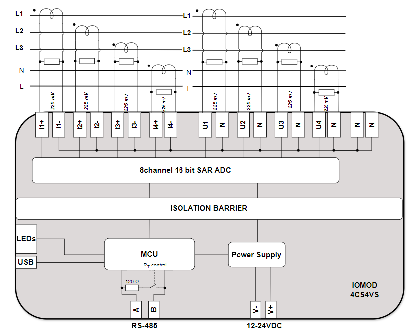
Fig. 1.2.1 IOMod 4Cs4Vs internal structure and block diagram
2. Hardware data
2.1 Mechanical drawings

Fig. 2.1.1 IOMod 4Cs4Vs side view with dimensions and terminal description.
1 – current measurement inputs; 2 – voltage measurement inputs;
3 – ground input for analogue measurements; 4 - RS485 interface;
5 - power supply input

Fig. 2.1.2 IOMod 4Cs4Vs front view with dimensions
2.2 Terminal Connections
IOMod 4Cs4Vs has 22 terminals, which are depicted below:

Fig. 2.2.1 IOMod 4Cs4Vs terminal diagram
The description of each terminal can be found in the table below:
Table 2.2.1 Terminal Specifications
|
Terminal number |
Terminal name |
Description |
|
1 |
I1+ |
Current inputs |
|
2 |
I1- |
|
|
3 |
I2+ |
|
|
4 |
I2- |
|
|
5 |
I3+ |
|
|
6 |
I3- |
|
|
7 |
IN+ |
|
|
8 |
IN- |
|
|
9 |
U1 |
Voltage inputs |
|
10 |
N |
|
|
11 |
U2 |
|
|
12 |
N |
|
|
13 |
U3 |
|
|
14 |
N |
|
|
15 |
U4 |
|
|
16 |
N |
|
|
17 |
N |
Common |
|
18 |
N |
|
|
19 |
A |
RS485 input |
|
20 |
B̄ |
|
|
21 |
V- |
Power source input |
|
22 |
V+ |
2.3 Status indication
IOMod 4Cs4Vs have 2 LEDs (Fig. 2.3.1), which indicate communication and power statuses.

Fig. 2.3.1 IOMod 4Cs4Vs LEDs physical location
The description of each IOMod 4Cs4Vs LED can be found in the table below:
Table 2.3.1 Description of LEDs.
|
Name |
LED color |
Description |
|
RX/TX |
🟢 (green) |
A blinking green light indicates active communication via the RS485 interface. |
|
STAT |
🟢 (green) |
The power source is connected to the power supply input. |
|
🔵 (blue) |
IOMod Meter is connected to an external device via a USB mini cable. |
3. Technical information
Table 3.1 Technical specifications.
|
System |
||
|
1. |
Dimension |
101 x 119 x 17.5 mm |
|
2. |
Case |
ABS, black |
|
3. |
Working environment |
Indoor |
|
4. |
Working temperature |
From -40°C to +85°C |
|
5. |
Recommended operating conditions |
5 – 60°C and 20 – 80%RH |
|
6. |
Configuration |
USB – configuration via IOMod Utility RS485 – configuration via IOMod Utility |
|
7. |
Firmware upgrade |
USB – IOMod Utility RS485 - IOMod Utility |
|
Electrical specifications |
||
|
8. |
Inputs |
16-bit resolution, Input resistance: ~1 MOhm Input capacitance: ~170 pF Input Ranges: ±10 V (amplitude); Nominal values:
Overvoltage protection of all inputs up to ±20 V (amplitude) |
|
Power |
||
|
9. |
Power Supply |
9 V to 33 V |
|
10. |
Current consumption |
40 mA @ 12 VDC, 20 mA @ 24 VDC |
4. Mounting and Installation
4.1 Connection Diagrams
This chapter discusses the various options for connecting the device to medium-voltage systems.
4.1.1 IOMod 4Cs4Vs connection for two feeders
The special feature of IOMod 4Cs4Vs is the ability to be used for two feeders (Fig 4.1.1.1). In this case, the 4I4I connection mode needs to be enabled in IOMod Utility (Fig. 4.1.1.2).
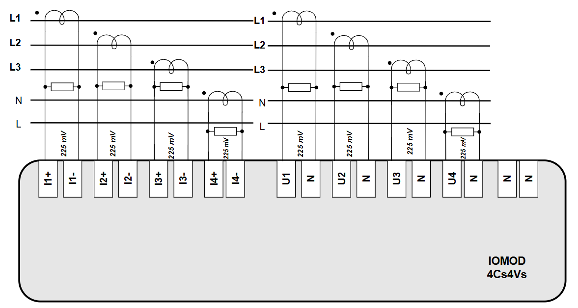
Fig. 4.1.1.1 IOMod 4Cs4Vs connection diagram for feeders

Fig. 4.1.1.2 IOMod Utility General settings tab with Connection mode set to 4I4I
This mode allows us to use IOMod 4Cs4Vs voltage inputs for current measurements so that the currents of both feeders are measured simultaneously. In the connection scheme above (Fig. 4.1.1.1) IOMod 4Cs4Vs current inputs are connected to the pair of feeders via low-power current sensors.
4.1.2 3 Low-Power Voltage Sensor, 2-Phase Current, and Core Balance Current Transformer
IOMod 4Cs4Vs allow directly measuring the neutral current. To use this feature I0 current acquiring mode needs to be switched in IOMod Utility from calculated to metered (Fig. 4.1.2.1).
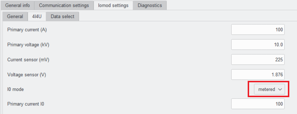
Fig. 4.1.2.1 IOMod Utility 4I4U settings view with I0 mode switched to metered
After enabling I0 metered mode IOMod 4Cs4Vs second phase input (I2+/I2-) becomes neutral current input. Since neutral current measurements are performed directly instead of being calculated it allows to achieve much higher precision and sensitivity. While the neutral current is being metered directly, the second phase measurements are being calculated by taking a vector sum of the measured currents. In the scheme below (Fig. 4.1.2.2) current and voltage measurements are taken by using low-power current and low-power voltage sensors. The second input (I2+/I2-) is connected to a low-power current sensor which is placed on the neutral line.
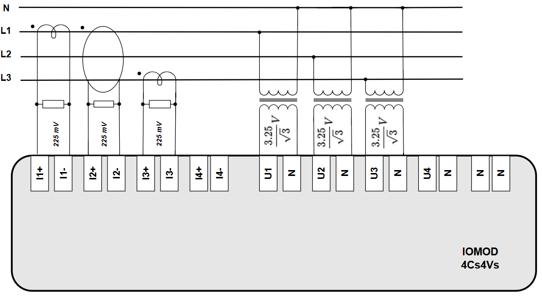
Fig. 4.1.2.2 IOMod 4Cs4Vs I0 metered mode connection diagram
4.1.3 2 Phase Current, and Core Balance Current Transformer
Similarly to the I0 calculated mode, IOMod 4Cs4Vs can take solely current measurements via low-power current sensors (Fig. 4.1.3.1). However, this connection scheme restricts IOMod FPI fault detection capabilities only to the current-related faults. Also, the absence of voltage measurements results in an inability to provide the directional fault information.
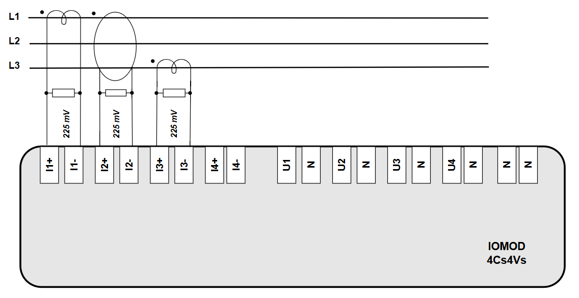
Fig. 4.1.3.1 IOMod 4Cs4Vs I0 metered mode connection diagram without voltage measurements
4.2 Power Supply
IOMod 4Cs4Vs need to be powered by a 9–33 V power source. IOMod 4Cs4Vs power supply inputs are located next to RS485 interface inputs (Fig 4.3.1).

Fig. 4.3.1 Power supply inputs physical location
4.3 USB Connection
IOMod 4Cs4Vs device has a USB-mini connection port. Its primary function is the physical connection establishment between the IOMod and a PC. By selecting the USB interface and correct communication port in IOMod Utility (Fig. 4.4.1) a user can connect to the IOMod to control its parameters and monitor its measured data and the status of fault detection functions. Also, this connection can be used for powering the module.

Fig. 4.4.1 IOMod Utility interface and communication port parameters

Fig. 4.4.2 IOMod 4Cs4Vs USB connection port physical location
5. Parametrization
In this section, the IOMod 4Cs4Vs settings configuration is described. IOMod 4Cs4Vs configuration is performed via IOMod Utility (the manual can be accessed here). All IOMod-related settings can be found in the "IOMod settings" tab (Fig. 5.1).
![]()
Fig. 5.1 IOMod settings tab
5.1 General Parameters
To configure IOMod 4Cs4Vs general settings open the "IOMod settings" tab in IOMod Utility. After clicking on "IOMod settings", the "General" section opens (Fig. 5.1.1).

Fig. 5.1.1 IOMod Utility with IOMod 4Cs4Vs general settings window opened
The general settings consist of two parameters, which apply to all communication protocols (Table 5.1.1). "Measurands set" and "Scale factor" are defined only in the context of the IEC 60870-5-103 communication protocol. The last parameter "Value update time (ms)" is defined only in the context of IEC 60870-5-101 and IEC 60870-5-103 communication protocols.
Table 5.1.1 IOMod 4Cs4Vs general parameter ranges and default values.
|
Parameter |
Range |
Default value |
|
Connection mode |
4I4I, 4I4U |
4I4I |
|
Frequency |
50 Hz, 60 Hz |
50 Hz |
|
Value update time (ms) * |
20-60000 |
500 |
|
Measurands set ** |
1-4 |
1 |
|
Scale factor ** |
1.2, 1.4 |
1.2 |
*The parameter is defined only for IEC 60870-5-101 and IEC 60870-5-103 communication protocols.
** The parameters are defined only for the IEC 60870-5-103 communication protocol.
The first parameter "Connection mode" allows us to define how the values measured with voltage inputs (terminals 9–16, see Fig. 2.2.1) are supposed to be interpreted. The values are interpreted as voltage measurements by default. This connection mode is denoted by the 4I4U designation. 4I4U designation means – "4 currents and 4 voltages" meaning that both current and voltage measurements are being taken from a feeder. 4I4U connection mode parameters can be found in a separate settings section which is labelled with communication mode designation (connection mode settings are described in the next section).
Selecting 4I4I connection mode in IOMod Utility changes IOMod Setting sections – 4I4U changes to 4I4I. IOMod 4Cs4Vs, in 4I4I connection mode, interprets the values measured with voltage inputs (terminals 9–16, see Fig. 2.2.1) as current measurements. 4I4I designation means – "4 currents and 4 currents" meaning that the voltage inputs become the second channel current inputs. The 4I4I settings section allows us to modify connection mode parameters (described in the next section).
The "Frequency" parameter allows us to set the nominal frequency of the power line to which IOMod 4Cs4Vs is connected.
If the IEC 60870-5-103 communication protocol is selected, the "Measurands set" parameter sets one of the lists of measurements (Table 6.3.2, Table 6.3.3) which is going to be sent to a master device.
If the IEC 60870-5-103 communication protocol is selected, the "Scale factor" parameter sets a value by which all measurements are going to be multiplied.
The value update time (ms) parameter defines how frequently the updated values are going to be sent to a controlling station via IEC 60870-5-101 or IEC 60870-5-103 communication protocols.
5.2 Connection mode settings
As was described early IOMod 4Cs4Vs supports two connection modes – 4I4U and 4I4I. After selecting one of them in General settings (Fig. 5.1.1) a new respectively named section appears. In this subsection, the parameters of a certain connection mode are going to be described.
5.2.1 4I4U connection mode parameters
The 4I4U connection mode parameters section has six parameters (Table 5.2), which are going to be described below.
Table 5.2 4I4U connection mode parameters.
|
Parameter |
Range |
Default value |
|
Primary current (A) |
1–2000 |
100 |
|
Primary voltage (kV) |
0.2–60.0 |
10.0 |
|
Current sensor (mV) |
100–300 |
225 |
|
Voltage sensor (V) |
1.0–3.0 |
1.876 |
|
I0 mode |
Calculated, Metered |
Calculated |
|
Primary current I0 |
1–2000 |
100 |
- The "Primary current (A)" parameter defines the nominal input current of a current sensor or a current transformer.
- The "Primary voltage (kV)" parameter sets the nominal input line voltage of a voltage sensor or a voltage transformer. If instead of the line voltage, the sensor or adapter converts the phase voltage, still the value of the line voltage must be used. For example, if a voltage sensor declares the primary voltage of 10/√3 kV, then 10 kV must be used for the "Primary voltage (kV)" parameter, for it is the line voltage of the network.
- The "Current sensor (mV)" parameter defines the nominal output voltage of a current sensor or a current transformer.
- The "Voltage sensor (V)" parameter defines the nominal output phase voltage of a voltage sensor or a voltage transformer. Contrary to the Primary Voltage, the phase voltage must be used for this parameter. For example, if a voltage sensor declares the secondary voltage of 3.25/√3 V, then the approximate phase voltage value must be used. It means, that the given expression must be evaluated (3.25/√3 ≈ 1.876 V) and the result must be entered into the "Voltage sensor (V)" parameter (1.876 V).
- The "I0 mode" parameter defines the way of obtaining the neutral current values. The default parameter value is "Calculated", meaning that the value of the neutral current is going to be calculated by taking the phase current measurements. If "Metered" is selected, then the neutral current values are expected to be measured directly.
- The "Primary current I0" parameter defines the nominal input neutral current which is being measured by a Core Balance Current Transformer.
5.2.2 4I4I connection mode parameters
The 4I4I connection mode parameters section has eight parameters (Table 5.3), which are going to be described below.
Table 5.3 4I4I connection mode parameters.
|
Parameter |
Range |
Default value |
|
Primary current ch1 (A) |
1–2000 |
100 |
|
Primary current ch2 (A) |
1–2000 |
100 |
|
Current sensor ch1 (mV) |
100–300 |
225 |
|
Current sensor ch2 (mV) |
100–300 |
225 |
|
I0 mode ch1 |
Calculated, Metered |
Calculated |
|
I0 mode ch2 |
Calculated, Metered |
Calculated |
|
Primary current I0 ch1 |
1–2000 |
100 |
|
Primary current I0 ch2 |
1–2000 |
100 |
- The "Primary current ch1 (A)" parameter sets the nominal input current of a current sensor or a current transformer which is connected to the first channel current inputs.
- The "Primary current ch2 (A)" parameter sets the nominal input current of a current sensor or a current transformer which is connected to the second channel current inputs.
- The "Current sensor ch1 (mV)" parameter defines the nominal output voltage of a current sensor or a current transformer which is connected to the first channel current inputs.
- The "Current sensor ch2 (mV)" parameter defines the nominal output voltage of a current sensor or a current transformer which is connected to the second channel current inputs.
- The "I0 mode ch1" parameter defines the way of obtaining the neutral current values with the first channel current inputs. The default parameter value is "Calculated", meaning that the value of the neutral current is going to be calculated by taking the phase current measurements. If "Metered" is selected, then the neutral current values are expected to be measured directly.
- The "I0 mode ch2" parameter defines the way of obtaining the neutral current values with the second channel current inputs. The default parameter value is "Calculated", meaning that the value of the neutral current is going to be calculated by taking the phase current measurements. If "Metered" is selected, then the neutral current values are expected to be measured directly.
- The "Primary current I0 ch1" parameter defines the nominal input neutral current which is being measured by a Core Balance Current Transformer connected to the first channel current inputs.
- The "Primary current I0 ch2" parameter defines the nominal input neutral current which is being measured by a Core Balance Current Transformer connected to the second channel current inputs.
5.3 Data Select
The data select tab (Fig. 5.3.1) is the last IOMod settings section, which provides a way to control the data being sent via the IEC 60870-5-101 communication protocol. The IOA (Information Object Address) of each data unit is specified in the brackets to the right of a parameter's name. To include a parameter to a set of parameters which are sent via IEC 60870-5-101 communication protocol a checkbox to the right of a parameter's name needs to be checked.

Fig. 5.3.1 IOMod 4Cs4Vs Data select tab view
5.4 Diagnostics
The IOMod Utility Diagnostics tab allows real-time monitoring of IOMod 4Cs4Vs measurements and harmonics statuses. The diagnostics mode of both measurements and harmonics is turned off by default. This is indicated by the red "Offline" word designation and by the unchanging black circle (Fig. 5.4.1, Fig. 5.4.2).
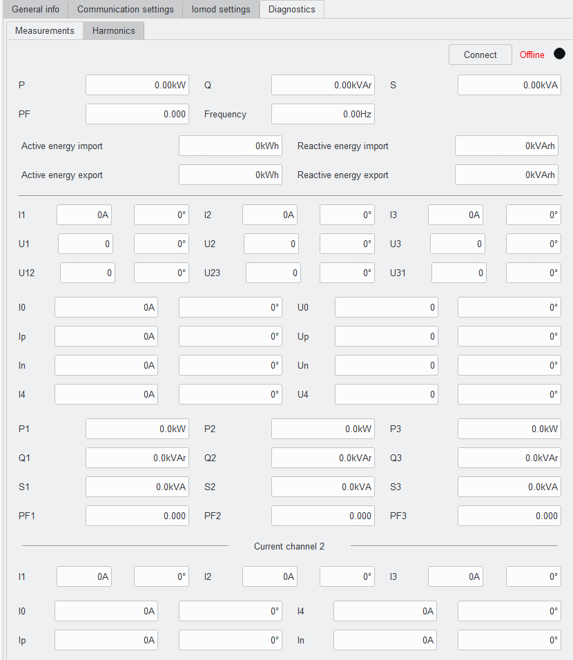
Fig. 5.4.1 IOMod Utility Diagnostics tab Measurements section in offline mode
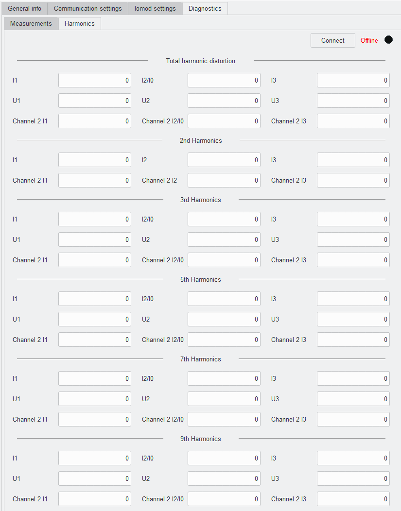
Fig. 5.4.2 IOMod Utility DIganostics tab Harmonics section in offline mode
To turn on real-time monitoring of both Diagnostics sections, the "Connect" button to the left of the "Offline" word designation needs to be pressed. The button can be pressed in either the Diagnostics sections (Measurements or Harmonics). After pressing the "Connect" button the word designation of Diagnostics mode changes to "Online", the black circle starts blinking and the button name changes to "Disconnect".
It is advisable to turn off Diagnostics mode before setting new IOMod 4Cs4Vs parameters. To turn off Diagnostics real-time monitoring mode, the "Disconnect" button needs to be pressed.
6. Communication Protocols
IOMod 4Cs4Vs supports three communication protocols: Modbus RTU, IEC 60870-5-101 and IEC 60870-5-103. Using these communication protocols a user via a master device can read the measured data from the device. The communication protocol can be selected using IOMod Utility (IOMod Utility manual can be accessed here).
6.1 Modbus RTU operational information
When the Modbus RTU protocol is selected IOMod 4Cs4Vs acts as a slave device and waits for requests from the Modbus master. For reading the measurements, a master can send a Read Input Register (FC 04) request. Request with an unsupported function code or register number out of range will be answered with the corresponding exception. Measurement results in nominal values having an integer type, while results in primary values are 32-bit float type.
Table 6.1.1 Nominal values in integer format. The data can be read using Modbus FC4 request.
|
Address (Dec) |
Description |
Units |
Data type |
Access |
|
0 |
Phase L1 current |
% x10 |
UINT16 |
R |
|
1 |
Phase L2 current |
% x10 |
UINT16 |
R |
|
2 |
Phase L3 current |
% x10 |
UINT16 |
R |
|
3 |
Calculated neutral current |
% x10 |
UINT16 |
R |
|
4 |
Calculated line voltage U12 |
% x10 |
UINT16 |
R |
|
5 |
Calculated line voltage U23 |
% x10 |
UINT16 |
R |
|
6 |
Calculated line voltage U31 |
% x10 |
UINT16 |
R |
|
7 |
Calculated zero sequence voltage |
% x10 |
UINT16 |
R |
|
8 |
Total 3 phase apparent power (S1+S2+S3) |
% x10 |
UINT16 |
R |
|
9 |
Total 3 phase active power (P1+P2+P3) |
% x10 |
INT16 |
R |
|
10 |
Total 3 phase reactive power (Q1+Q2+Q3) |
% x10 |
INT16 |
R |
|
11 |
Total 3-phase power factor |
x1000 |
INT16 |
R |
|
12 |
Total harmonic distortions of U1 voltage |
UINT16 |
R |
|
|
13 |
Total harmonic distortions of U2 voltage |
UINT16 |
R |
|
|
14 |
Total harmonic distortions of U3 voltage |
UINT16 |
R |
|
|
15 |
Total harmonic distortions of I1 current |
UINT16 |
R |
|
|
16 |
Total harmonic distortions of I2 current |
UINT16 |
R |
|
|
17 |
Total harmonic distortions of I3 current |
UINT16 |
R |
|
|
18 |
3rd harmonic level of the I1 current |
% |
UINT16 |
R |
|
19 |
5th harmonic level of I1 current |
% |
UINT16 |
R |
|
20 |
7th harmonic level of I1 current |
% |
UINT16 |
R |
|
21 |
9th harmonic level of I1 current |
% |
UINT16 |
R |
|
22 |
3rd harmonic level of the I2 current |
% |
UINT16 |
R |
|
23 |
5th harmonic level of I2 current |
% |
UINT16 |
R |
|
24 |
7th harmonic level of I2 current |
% |
UINT16 |
R |
|
25 |
9th harmonic level of I2 current |
% |
UINT16 |
R |
|
26 |
3rd harmonic level of the I3 current |
% |
UINT16 |
R |
|
27 |
5th harmonic level of I3 current |
% |
UINT16 |
R |
|
28 |
7th harmonic level of I3 current |
% |
UINT16 |
R |
|
29 |
9th harmonic level of I3 current |
% |
UINT16 |
R |
|
30 |
3rd harmonic level of U1 voltage |
% |
UINT16 |
R |
|
31 |
5th harmonic level of U1 voltage |
% |
UINT16 |
R |
|
32 |
7th harmonic level of U1 voltage |
% |
UINT16 |
R |
|
33 |
9th harmonic level of U1 voltage |
% |
UINT16 |
R |
|
34 |
3rd harmonic level of U2 voltage |
% |
UINT16 |
R |
|
35 |
5th harmonic level of U2 voltage |
% |
UINT16 |
R |
|
36 |
7th harmonic level of U2 voltage |
% |
UINT16 |
R |
|
37 |
9th harmonic level of U2 voltage |
% |
UINT16 |
R |
|
38 |
3rd harmonic level of U3 voltage |
% |
UINT16 |
R |
|
39 |
5th harmonic level of U3 voltage |
% |
UINT16 |
R |
|
40 |
7th harmonic level of U3 voltage |
% |
UINT16 |
R |
|
41 |
9th harmonic level of U3 voltage |
% |
UINT16 |
R |
|
42 |
Phase L1 active power |
% x10 |
INT16 |
R |
|
43 |
Phase L2 active power |
% x10 |
INT16 |
R |
|
44 |
Phase L3 active power |
% x10 |
INT16 |
R |
|
45 |
Phase L1 reactive power |
% x10 |
INT16 |
R |
|
46 |
Phase L2 reactive power |
% x10 |
INT16 |
R |
|
47 |
Phase L3 reactive power |
% x10 |
INT16 |
R |
|
48 |
The phase angle of U1 voltage |
0.1 deg |
INT16 |
R |
|
49 |
The phase angle of U2 voltage |
0.1 deg |
INT16 |
R |
|
50 |
The phase angle of U3 voltage |
0.1 deg |
INT16 |
R |
|
51 |
Phase L1 voltage |
% x10 |
UINT16 |
R |
|
52 |
Phase L2 voltage |
% x10 |
UINT16 |
R |
|
53 |
Phase L3 voltage |
% x10 |
UINT16 |
R |
|
54 |
Frequency of phase L1 voltage |
Hz x100 |
UINT16 |
R |
|
55 |
Input I4 current |
% x10 |
UINT16 |
R |
|
56 |
Input U4 voltage |
% x10 |
UINT16 |
R |
|
57 |
S1 phase apparent power |
% x10 |
INT16 |
R |
|
58 |
S2 phase apparent power |
% x10 |
INT16 |
R |
|
59 |
S3 phase apparent power |
% x10 |
INT16 |
R |
|
60 |
L1 phase power factor |
% x10 |
INT16 |
R |
|
61 |
L2 phase power factor |
% x10 |
INT16 |
R |
|
62 |
L3 phase power factor |
% x10 |
INT16 |
R |
|
63 |
The angle of the I1 current |
0.1 deg |
INT16 |
R |
|
64 |
The angle of the I2 current |
0.1 deg |
INT16 |
R |
|
65 |
The angle of the I3 current |
0.1 deg |
INT16 |
R |
|
66 |
Line voltage U12 angle |
0.1 deg |
INT16 |
R |
|
67 |
Line voltage U23 angle |
0.1 deg |
INT16 |
R |
|
68 |
Line voltage U31 angle |
0.1 deg |
INT16 |
R |
|
69 |
Current positive sequence |
Data * 10 |
UINT16 |
% |
|
70 |
Current negative sequence |
% x10 |
UINT16 |
R |
|
71 |
Voltage positive sequence |
% x10 |
UINT16 |
R |
|
72 |
Voltage negative sequence |
% x10 |
UINT16 |
R |
|
73 |
Current I0 angle |
0.1 deg |
UINT16 |
R |
|
74 |
Current I4 angle |
0.1 deg |
UINT16 |
R |
|
75 |
Voltage U0 angle |
0.1 deg |
UINT16 |
R |
|
76 |
Voltage U4 angle |
0.1 deg |
UINT16 |
R |
|
77 |
Current Ip angle |
0.1 deg |
UINT16 |
R |
|
78 |
Current In angle |
0.1 deg |
UINT16 |
R |
|
79 |
Current Up angle |
0.1 deg |
UINT16 |
R |
|
80 |
Current Un angle |
0.1 deg |
UINT16 |
R |
|
81 |
Current I1 2nd harmonic |
% x10 |
UINT16 |
R |
|
82 |
Current I2 2nd harmonic |
% x10 |
UINT16 |
R |
|
83 |
Current I3 2nd harmonic |
% x10 |
UINT16 |
R |
|
84 |
Current I1 channel 2 |
% x10 |
UINT16 |
R |
|
85 |
Current I2 channel 2 |
% x10 |
UINT16 |
R |
|
86 |
Current I3 channel 2 |
% x10 |
UINT16 |
R |
|
87 |
Current I0 channel 2 |
% x10 |
UINT16 |
R |
|
88 |
Current I4 channel 2 |
% x10 |
UINT16 |
R |
|
89 |
Current Ip channel 2 |
% x10 |
UINT16 |
R |
|
90 |
Current In channel 2 |
% x10 |
UINT16 |
R |
|
91 |
Current I1 channel 2 angle |
0.1 deg |
UINT16 |
R |
|
92 |
Current I2 channel 2 angle |
0.1 deg |
UINT16 |
R |
|
93 |
Current I3 channel 2 angle |
0.1 deg |
UINT16 |
R |
|
94 |
Current I0 channel 2 angle |
0.1 deg |
UINT16 |
R |
|
95 |
Current I4 channel 2 angle |
0.1 deg |
UINT16 |
R |
|
96 |
Current Ip channel 2 angle |
0.1 deg |
UINT16 |
R |
|
97 |
Current In channel 2 angle |
0.1 deg |
UINT16 |
R |
|
98 |
Current I1 2nd harmonic channel 2 |
0.1 deg |
UINT16 |
R |
|
99 |
Current I2 2nd harmonic channel 2 |
0.1 deg |
UINT16 |
R |
|
100 |
Current I3 2nd harmonic channel 2 |
0.1 deg |
UINT16 |
R |
|
101 |
THD of current I1 channel 2 |
UINT16 |
R |
|
|
102 |
THD of current I2 channel 2 |
UINT16 |
R |
|
|
103 |
THD of current I3 channel 2 |
UINT16 |
R |
|
|
104 |
Current I1 3rd harmonic channel 2 |
% |
UINT16 |
R |
|
105 |
Current I1 5th harmonic channel 2 |
% |
UINT16 |
R |
|
106 |
Current I1 7th harmonic channel 2 |
% |
UINT16 |
R |
|
107 |
Current I1 9th harmonic channel 2 |
% |
UINT16 |
R |
|
108 |
Current I2 3rd harmonic channel 2 |
% |
UINT16 |
R |
|
109 |
Current I2 5th harmonic channel 2 |
% |
UINT16 |
R |
|
110 |
Current I2 7th hamonic channel 2 |
% |
UINT16 |
R |
|
111 |
Current I2 9th harmonic channel 2 |
% |
UINT16 |
R |
|
112 |
Current I3 3rd harmonic channel 2 |
% |
UINT16 |
R |
|
113 |
Current I3 5th harmonic channel 2 |
% |
UINT16 |
R |
|
114 |
Current I3 7th harmonic channel 2 |
% |
UINT16 |
R |
|
115 |
Current I3 9th harmonic channel 2 |
% |
UINT16 |
R |
|
116-117 |
Active import energy |
kWh |
UINT32 |
R |
|
118-119 |
Active export energy |
kWh |
UINT32 |
R |
|
120-121 |
Reactive import energy |
kVArh |
UINT32 |
R |
|
122-123 |
Reactive export energy |
kVArh |
UINT32 |
R |
Table 6.1.2 Primary values in float format. The data can be read using Modbus FC4.
|
Address (Dec) |
Description |
Units |
Data type |
Access |
|
200 - 201 |
Current I1 |
A |
FLOAT |
R |
|
202 - 203 |
Current I2 |
A |
FLOAT |
R |
|
204 - 205 |
Current I3 |
A |
FLOAT |
R |
|
206 - 207 |
Current I0 |
A |
FLOAT |
R |
|
208 - 209 |
Voltage U12 |
U |
FLOAT |
R |
|
210 - 211 |
Voltage U23 |
U |
FLOAT |
R |
|
212 - 213 |
Voltage U31 |
U |
FLOAT |
R |
|
214 - 215 |
Voltage U1 |
U |
FLOAT |
R |
|
216 - 217 |
Voltage U2 |
U |
FLOAT |
R |
|
218 - 219 |
Voltage U3 |
U |
FLOAT |
R |
|
220 - 221 |
Voltage U0 |
U |
FLOAT |
R |
|
222 - 223 |
Voltage U1 angle |
° |
FLOAT |
R |
|
224 - 225 |
Voltage U2 angle |
° |
FLOAT |
R |
|
226 - 227 |
Voltage U3 angle |
° |
FLOAT |
R |
|
228 - 229 |
Apparent power Σ 3 phase |
VA |
FLOAT |
R |
|
230 - 231 |
Active power Σ 3 phase |
W |
FLOAT |
R |
|
232 - 233 |
Reactive power Σ 3 phase |
Var |
FLOAT |
R |
|
234 - 235 |
Power factor Σ 3 phase |
FLOAT |
R |
|
|
236 - 237 |
Apparent power S1 |
VA |
FLOAT |
R |
|
238 - 239 |
Apparent power S2 |
VA |
FLOAT |
R |
|
240 - 241 |
Apparent power S3 |
VA |
FLOAT |
R |
|
242 - 243 |
Active power P1 |
W |
FLOAT |
R |
|
244 - 245 |
Active power P2 |
W |
FLOAT |
R |
|
246 - 247 |
Active power P3 |
W |
FLOAT |
R |
|
248 - 249 |
Reactive power Q1 |
Var |
FLOAT |
R |
|
250 - 251 |
Reactive power Q2 |
Var |
FLOAT |
R |
|
252 - 253 |
Reactive power Q3 |
Var |
FLOAT |
R |
|
254 - 255 |
Power factor PF1 |
FLOAT |
R |
|
|
256 - 257 |
Power factor PF2 |
FLOAT |
R |
|
|
258 - 259 |
Power factor PF3 |
FLOAT |
R |
|
|
260 - 261 |
Frequency |
Hz |
FLOAT |
R |
|
262 - 263 |
THD Voltage U1 |
FLOAT |
R |
|
|
264 - 265 |
THD Voltage U2 |
FLOAT |
R |
|
|
266 - 267 |
THD Voltage U3 |
FLOAT |
R |
|
|
268 - 269 |
THD Current I1 |
FLOAT |
R |
|
|
270 - 271 |
THD Current I2 |
FLOAT |
R |
|
|
272 - 273 |
THD Current I3 |
FLOAT |
R |
|
|
274 - 275 |
Current I1 3rd harmonic |
FLOAT |
R |
|
|
276 - 277 |
Current I1 5th harmonic |
FLOAT |
R |
|
|
278 - 279 |
Current I1 7th harmonic |
FLOAT |
R |
|
|
280 - 281 |
Current I1 9th harmonic |
FLOAT |
R |
|
|
282 - 283 |
Current I2 3rd harmonic |
FLOAT |
R |
|
|
284 - 285 |
Current I2 5th harmonic |
FLOAT |
R |
|
|
286 - 287 |
Current I2 7th harmonic |
FLOAT |
R |
|
|
288 - 289 |
Current I2 9th harmonic |
FLOAT |
R |
|
|
290 - 291 |
Current I3 3rd harmonic |
FLOAT |
R |
|
|
292 - 293 |
Current I3 5th harmonic |
FLOAT |
R |
|
|
294 - 295 |
Current I3 7th harmonic |
FLOAT |
R |
|
|
296 - 297 |
Current I3 9th harmonic |
FLOAT |
R |
|
|
298 - 299 |
Voltage U1 3rd harmonic |
FLOAT |
R |
|
|
300 - 301 |
Voltage U1 5th harmonic |
FLOAT |
R |
|
|
302 - 303 |
Voltage U1 7th harmonic |
FLOAT |
R |
|
|
304 - 305 |
Voltage U1 9th harmonic |
FLOAT |
R |
|
|
306 - 307 |
Voltage U2 3rd harmonic |
FLOAT |
R |
|
|
308 - 309 |
Voltage U2 5th harmonic |
FLOAT |
R |
|
|
310 - 311 |
Voltage U2 7th harmonic |
FLOAT |
R |
|
|
312 - 313 |
Voltage U2 9th harmonic |
FLOAT |
R |
|
|
314 - 315 |
Voltage U3 3rd harmonic |
FLOAT |
R |
|
|
316 - 317 |
Voltage U3 5th harmonic |
FLOAT |
R |
|
|
318 - 319 |
Voltage U3 7th harmonic |
FLOAT |
R |
|
|
320 - 321 |
Voltage U3 9th harmonic |
FLOAT |
R |
|
|
322 - 323 |
Current I4 |
A |
FLOAT |
R |
|
324 - 325 |
Voltage U4 |
U |
FLOAT |
R |
|
326 - 327 |
Current I1 angle |
° |
FLOAT |
R |
|
328 - 329 |
Current I2 angle |
° |
FLOAT |
R |
|
330 - 331 |
Current I3 angle |
° |
FLOAT |
R |
|
332 - 333 |
Current I0 angle |
° |
FLOAT |
R |
|
334 - 335 |
Voltage U0 angle |
° |
FLOAT |
R |
|
336 - 337 |
Voltage U12 angle |
° |
FLOAT |
R |
|
338 - 339 |
Voltage U23 angle |
° |
FLOAT |
R |
|
340 - 341 |
Voltage U31 angle |
° |
FLOAT |
R |
|
342 - 343 |
Current I4 angle |
° |
FLOAT |
R |
|
344 - 345 |
Voltage U4 angle |
° |
FLOAT |
R |
|
346 - 347 |
Current positive seq Ip |
A |
FLOAT |
R |
|
348 - 349 |
Current negative seq In |
A |
FLOAT |
R |
|
350 - 351 |
Current Ip angle |
° |
FLOAT |
R |
|
352 - 353 |
Current In angle |
° |
FLOAT |
R |
|
354 - 355 |
Voltage positive seq Up |
U |
FLOAT |
R |
|
356 - 357 |
Voltage negative seq Un |
U |
FLOAT |
R |
|
358 - 359 |
Voltage Up angle |
° |
FLOAT |
R |
|
360 - 361 |
Voltage Un angle |
° |
FLOAT |
R |
|
362 - 363 |
Current I1 2nd harmonic |
FLOAT |
R |
|
|
364 - 365 |
Current I2 2nd harmonic |
FLOAT |
R |
|
|
366 - 367 |
Current I3 2nd harmonic |
FLOAT |
R |
|
|
368 - 369 |
Current I1 channel 2 |
A |
FLOAT |
R |
|
370 - 371 |
Current I2 channel 2 |
A |
FLOAT |
R |
|
372 - 373 |
Current I3 channel 2 |
A |
FLOAT |
R |
|
374 - 375 |
Current I0 channel 2 |
A |
FLOAT |
R |
|
376 - 377 |
Current I4 channel 2 |
A |
FLOAT |
R |
|
378 - 379 |
Current I1 channel 2 angle |
° |
FLOAT |
R |
|
380 - 381 |
Current I2 channel 2 angle |
° |
FLOAT |
R |
|
382 - 383 |
Current I3 channel 2 angle |
° |
FLOAT |
R |
|
384 - 385 |
Current I0 channel 2 angle |
° |
FLOAT |
R |
|
386 - 387 |
Current I4 channel 2 angle |
° |
FLOAT |
R |
|
388 - 389 |
Current Ip channel 2 |
A |
FLOAT |
R |
|
390 - 391 |
Current In channel 2 |
A |
FLOAT |
R |
|
392 - 393 |
Current Ip channel 2 angle |
° |
FLOAT |
R |
|
394 - 395 |
Current In channel 2 angle |
° |
FLOAT |
R |
|
396 - 397 |
Current I1 2nd harmonic ch2 |
FLOAT |
R |
|
|
398 - 399 |
Current I2 2nd harmonic ch2 |
FLOAT |
R |
|
|
400 - 401 |
Current I3 2nd harmonic ch2 |
FLOAT |
R |
|
|
402 - 403 |
THD Current I1 ch2 |
FLOAT |
R |
|
|
404 - 405 |
THD Current I2 ch2 |
FLOAT |
R |
|
|
406 - 407 |
THD Current I3 ch2 |
FLOAT |
R |
|
|
408 - 409 |
Current I1 3rd harmonic ch2 |
FLOAT |
R |
|
|
410 - 411 |
Current I1 5th harmonic ch2 |
FLOAT |
R |
|
|
412 - 413 |
Current I1 7th harmonic ch2 |
FLOAT |
R |
|
|
414 - 415 |
Current I1 9th harmonic ch2 |
FLOAT |
R |
|
|
416 - 417 |
Current I2 3rd harmonic ch2 |
FLOAT |
R |
|
|
418 - 419 |
Current I2 5th harmonic ch2 |
FLOAT |
R |
|
|
420 - 421 |
Current I2 7th harmonic ch2 |
FLOAT |
R |
|
|
422 - 423 |
Current I2 9th harmonic ch2 |
FLOAT |
R |
|
|
424 - 425 |
Current I3 3rd harmonic ch2 |
FLOAT |
R |
|
|
426 - 427 |
Current I3 5th harmonic ch2 |
FLOAT |
R |
|
|
428 - 429 |
Current I3 7th harmonic ch2 |
FLOAT |
R |
|
|
430 - 431 |
Current I3 9th harmonic ch2 |
FLOAT |
R |
6.2 IEC 60870-5-101 operational information
IEC 60870-5-101 (IEC101) is a communication protocol designed for telecontrol applications in power systems, enabling communication between a master station and slave devices (e.g., Remote Terminal Units or RTUs).
IOMod 4Cs4Vs via IEC101 protocol transmit various measurement signals in a standardized format. These signals are predefined in the IOMod and mapped to corresponding Information Object Addresses (IOA).
The protocol distinguishes between Type Identifiers (TI), which according to the standard define the format, structure and type of the data being sent. The status and measurement signals are assigned to two different Type Identifiers 7 and 13.
Time synchronization is critical for logging events. To synchronize time, the master sends a Time Sync command C_CS_NA_1 (103) with Cause of Transmission (COT) 6. According to the IEC 60870-5-101 protocol specification, time synchronization can be performed for multiple devices using broadcast messages. A master device sends a broadcast timesync command with a broadcast link address. This ensures consistent time-stamping for event recording and fault detection across the network.
All the measurements are represented in absolute values without any scaling and using standard units. Almost every measurement can be sent using 13 ("measured value, short floating-point number"). The measurements which are sent with TI 13 signals are not marked with timestamps. This is because these signals are not intended for spontaneous transmission upon a change, but rather are to be polled by a controlling (master) station. All energy measurements are assigned to the signals with TI 7, which stands for "bitstring of 32-bit". The necessity in other data formats for the energy measurements comes from the fact that they are saved in 32-bit unsigned integer data type. The usage of integer type instead of float ensures better precision.
Table 6.2.1 List of signals
|
IOA |
Description |
Units |
TI |
|
0 |
Current I1 |
A |
13 (M_ME_NC_1) |
|
1 |
Current I2 |
A |
13 (M_ME_NC_1) |
|
2 |
Current I3 |
A |
13 (M_ME_NC_1) |
|
3 |
Current I0 |
A |
13 (M_ME_NC_1) |
|
4 |
Voltage U12 |
U |
13 (M_ME_NC_1) |
|
5 |
Voltage U23 |
U |
13 (M_ME_NC_1) |
|
6 |
Voltage U31 |
U |
13 (M_ME_NC_1) |
|
7 |
Voltage U1 |
U |
13 (M_ME_NC_1) |
|
8 |
Voltage U2 |
U |
13 (M_ME_NC_1) |
|
9 |
Voltage U3 |
U |
13 (M_ME_NC_1) |
|
10 |
Voltage U0 |
U |
13 (M_ME_NC_1) |
|
11 |
Voltage U1 angle |
° |
13 (M_ME_NC_1) |
|
12 |
Voltage U2 angle |
° |
13 (M_ME_NC_1) |
|
13 |
Voltage U3 angle |
° |
13 (M_ME_NC_1) |
|
14 |
Apparent power Σ 3 phase |
VA |
13 (M_ME_NC_1) |
|
15 |
Active power Σ 3 phase |
W |
13 (M_ME_NC_1) |
|
16 |
Reactive power Σ 3 phase |
Var |
13 (M_ME_NC_1) |
|
17 |
Power factor Σ 3 phase |
13 (M_ME_NC_1) |
|
|
18 |
Apparent power S1 |
VA |
13 (M_ME_NC_1) |
|
19 |
Apparent power S2 |
VA |
13 (M_ME_NC_1) |
|
20 |
Apparent power S3 |
VA |
13 (M_ME_NC_1) |
|
21 |
Active power P1 |
W |
13 (M_ME_NC_1) |
|
22 |
Active power P2 |
W |
13 (M_ME_NC_1) |
|
23 |
Active power P3 |
W |
13 (M_ME_NC_1) |
|
24 |
Reactive power Q1 |
Var |
13 (M_ME_NC_1) |
|
25 |
Reactive power Q2 |
Var |
13 (M_ME_NC_1) |
|
26 |
Reactive power Q3 |
Var |
13 (M_ME_NC_1) |
|
27 |
Power factor PF1 |
13 (M_ME_NC_1) |
|
|
28 |
Power factor PF2 |
13 (M_ME_NC_1) |
|
|
29 |
Power factor PF3 |
13 (M_ME_NC_1) |
|
|
30 |
Frequency |
Hz |
13 (M_ME_NC_1) |
|
31 |
THD Voltage U1 |
13 (M_ME_NC_1) |
|
|
32 |
THD Voltage U2 |
13 (M_ME_NC_1) |
|
|
33 |
THD Voltage U3 |
13 (M_ME_NC_1) |
|
|
34 |
THD Current I1 |
13 (M_ME_NC_1) |
|
|
35 |
THD Current I2 |
13 (M_ME_NC_1) |
|
|
36 |
THD Current I3 |
13 (M_ME_NC_1) |
|
|
37 |
Current I1 3rd harmonic |
13 (M_ME_NC_1) |
|
|
38 |
Current I1 5th harmonic |
13 (M_ME_NC_1) |
|
|
39 |
Current I1 7th harmonic |
13 (M_ME_NC_1) |
|
|
40 |
Current I1 9th harmonic |
13 (M_ME_NC_1) |
|
|
41 |
Current I2 3rd harmonic |
13 (M_ME_NC_1) |
|
|
42 |
Current I2 5th harmonic |
13 (M_ME_NC_1) |
|
|
43 |
Current I2 7th harmonic |
13 (M_ME_NC_1) |
|
|
44 |
Current I2 9th harmonic |
13 (M_ME_NC_1) |
|
|
45 |
Current I3 3rd harmonic |
13 (M_ME_NC_1) |
|
|
46 |
Current I3 5th harmonic |
13 (M_ME_NC_1) |
|
|
47 |
Current I3 7th harmonic |
13 (M_ME_NC_1) |
|
|
48 |
Current I3 9th harmonic |
13 (M_ME_NC_1) |
|
|
49 |
Voltage U1 3rd harmonic |
13 (M_ME_NC_1) |
|
|
50 |
Voltage U1 5th harmonic |
13 (M_ME_NC_1) |
|
|
51 |
Voltage U1 7th harmonic |
13 (M_ME_NC_1) |
|
|
52 |
Voltage U1 9th harmonic |
13 (M_ME_NC_1) |
|
|
53 |
Voltage U2 3rd harmonic |
13 (M_ME_NC_1) |
|
|
54 |
Voltage U2 5th harmonic |
13 (M_ME_NC_1) |
|
|
55 |
Voltage U2 7th harmonic |
13 (M_ME_NC_1) |
|
|
56 |
Voltage U2 9th harmonic |
13 (M_ME_NC_1) |
|
|
57 |
Voltage U3 3rd harmonic |
13 (M_ME_NC_1) |
|
|
58 |
Voltage U3 5th harmonic |
13 (M_ME_NC_1) |
|
|
59 |
Voltage U3 7th harmonic |
13 (M_ME_NC_1) |
|
|
60 |
Voltage U3 9th harmonic |
13 (M_ME_NC_1) |
|
|
61 |
Current I4 |
A |
13 (M_ME_NC_1) |
|
62 |
Voltage U4 |
U |
13 (M_ME_NC_1) |
|
63 |
Current I1 angle |
° |
13 (M_ME_NC_1) |
|
64 |
Current I2 angle |
° |
13 (M_ME_NC_1) |
|
65 |
Current I3 angle |
° |
13 (M_ME_NC_1) |
|
66 |
Current I0 angle |
° |
13 (M_ME_NC_1) |
|
67 |
Voltage U0 angle |
° |
13 (M_ME_NC_1) |
|
68 |
Voltage U12 angle |
° |
13 (M_ME_NC_1) |
|
69 |
Voltage U23 angle |
° |
13 (M_ME_NC_1) |
|
70 |
Voltage U31 angle |
° |
13 (M_ME_NC_1) |
|
71 |
Current I4 angle |
° |
13 (M_ME_NC_1) |
|
72 |
Voltage U4 angle |
° |
13 (M_ME_NC_1) |
|
73 |
Current positive seq Ip |
A |
13 (M_ME_NC_1) |
|
74 |
Current negative seq In |
A |
13 (M_ME_NC_1) |
|
75 |
Current Ip angle |
° |
13 (M_ME_NC_1) |
|
76 |
Current In angle |
° |
13 (M_ME_NC_1) |
|
77 |
Voltage positive seq Up |
U |
13 (M_ME_NC_1) |
|
78 |
Voltage negative seq Un |
U |
13 (M_ME_NC_1) |
|
79 |
Voltage Up angle |
° |
13 (M_ME_NC_1) |
|
80 |
Voltage Un angle |
° |
13 (M_ME_NC_1) |
|
81 |
Current I1 2nd harmonic |
13 (M_ME_NC_1) |
|
|
82 |
Current I2 2nd harmonic |
13 (M_ME_NC_1) |
|
|
83 |
Current I3 2nd harmonic |
13 (M_ME_NC_1) |
|
|
84 |
Current I1 channel 2 |
A |
13 (M_ME_NC_1) |
|
85 |
Current I2 channel 2 |
A |
13 (M_ME_NC_1) |
|
86 |
Current I3 channel 2 |
A |
13 (M_ME_NC_1) |
|
87 |
Current I0 channel 2 |
A |
13 (M_ME_NC_1) |
|
88 |
Current I4 channel 2 |
A |
13 (M_ME_NC_1) |
|
89 |
Current I1 channel 2 angle |
° |
13 (M_ME_NC_1) |
|
90 |
Current I2 channel 2 angle |
° |
13 (M_ME_NC_1) |
|
91 |
Current I3 channel 2 angle |
° |
13 (M_ME_NC_1) |
|
92 |
Current I0 channel 2 angle |
° |
13 (M_ME_NC_1) |
|
93 |
Current I4 channel 2 angle |
° |
13 (M_ME_NC_1) |
|
94 |
Current Ip channel 2 |
A |
13 (M_ME_NC_1) |
|
95 |
Current In channel 2 |
A |
13 (M_ME_NC_1) |
|
96 |
Current Ip channel 2 angle |
° |
13 (M_ME_NC_1) |
|
97 |
Current In channel 2 angle |
° |
13 (M_ME_NC_1) |
|
98 |
Current I1 2nd harmonic ch2 |
13 (M_ME_NC_1) |
|
|
99 |
Current I2 2nd harmonic ch2 |
13 (M_ME_NC_1) |
|
|
100 |
Current I3 2nd harmonic ch2 |
13 (M_ME_NC_1) |
|
|
101 |
THD Current I1 ch2 |
13 (M_ME_NC_1) |
|
|
102 |
THD Current I2 ch2 |
13 (M_ME_NC_1) |
|
|
103 |
THD Current I3 ch2 |
13 (M_ME_NC_1) |
|
|
104 |
Current I1 3rd harmonic ch2 |
13 (M_ME_NC_1) |
|
|
105 |
Current I1 5th harmonic ch2 |
13 (M_ME_NC_1) |
|
|
106 |
Current I1 7th harmonic ch2 |
13 (M_ME_NC_1) |
|
|
107 |
Current I1 9th harmonic ch2 |
13 (M_ME_NC_1) |
|
|
108 |
Current I2 3rd harmonic ch2 |
13 (M_ME_NC_1) |
|
|
109 |
Current I2 5th harmonic ch2 |
13 (M_ME_NC_1) |
|
|
110 |
Current I2 7th harmonic ch2 |
13 (M_ME_NC_1) |
|
|
111 |
Current I2 9th harmonic ch2 |
13 (M_ME_NC_1) |
|
|
112 |
Current I3 3rd harmonic ch2 |
13 (M_ME_NC_1) |
|
|
113 |
Current I3 5th harmonic ch2 |
13 (M_ME_NC_1) |
|
|
114 |
Current I3 7th harmonic ch2 |
13 (M_ME_NC_1) |
|
|
115 |
Current I3 9th harmonic ch2 |
13 (M_ME_NC_1) |
|
|
400 |
Active import energy |
kWh |
7 (M_BO_NA_1) |
|
401 |
Active export energy |
kWh |
7 (M_BO_NA_1) |
|
402 |
Reactive import energy |
kVArh |
7 (M_BO_NA_1) |
|
403 |
Reactive export energy |
kVArh |
7 (M_BO_NA_1) |
6.3 IEC 60870-5-103 operational information
When the IEC-60870-5-103 protocol is selected IOMod uses a standard communication scheme. Initiation, control messages, and queries are initiated by a master (controlling station), while the IOMod device (controlled station) only answers requests and sends values. The first message sent by the master should be RESET CU to restart communication. When an acknowledge (ACK) packet is sent from a slave device, a master may proceed with acquiring General Interrogation and sending Time synchronization packets.
Time synchronization is critical for logging events. To synchronize time, the master sends a Time Sync command with function 0 and Cause of Transmission (COT) 8. According to the IEC 60870-5-103 protocol specification, time synchronization can be performed for multiple devices using broadcast messages. For broadcast time synchronization, the master device sends a periodic signal with a time stamp to synchronize the system time of slave devices. If synchronization fails, devices default to their local system time until they successfully resynchronize.
When this initialization is complete, the master should poll the IOMod device with Class 1 and Class 2 requests. Class 2 is used when the master polls for cyclic data. The controlled device responds when spontaneous data exists and the master then sends a request for Class 1. The controlled station responds with a time-tagged message.
As IOMod 4Cs4Vs does not have any digital inputs, only analog ones, therefore the general interrogation returns nothing. Values of measurements are returned cyclically as a response to Class 2 data requests.
Specific settings for the IEC 60870-5-103 protocol:
- Measurand set selection. A user can select which predefined measurand set will be transmitted to the host system. Available measurand sets are presented in table 6.3.1.
- Scale factor. The communication protocol IEC 60870-5-103 only lets 13-bit signed values in the range of -1...+1. When an IEC 60870-5-103 measurand, for example, phase voltage, is scaled as 2.4, it means that the measurand value 1 corresponds to 2.4×Un, the measurand value 0.5 corresponds to 1.2×In, and so on. If the measurand value, in this case, exceeds 2.4×Un, the IEC 60870-5-103 object value saturates at its maximum value and an overflow flag is set in the IEC 60870-5-103 object transmission.
- Device function type. By default, IOMod has IEC 60870-5-103 Function Type set to 253. If this Function type for some reason is not suitable – a user can define any other type
Table 6.3.1 Data sets for 4I4U connection mode
|
Set Nr. |
TYPE |
FUN* |
INF |
Qty of data |
Information elements (measurands) |
|
1 |
9 |
253 |
148 |
9 |
I1, I2, I3, U1, U2, U3, P, Q, f |
|
2 |
9 |
253 |
149 |
23 |
I1, I2, I3, I4, U1, U2, U3, U4, P1, P2, P3, Q1, Q2, Q3, S1, S2, S3, PF1, PF2, PF3, U12(angle), U23(angle), U13(angle) |
|
3 |
9 |
253 |
150 |
60 |
I1, I2, I3, IN, U1, U2, U3, UN, P1, P2, P3, Q1, Q2, Q3, S1, S2, S3, PF1, PF2, PF3, U12, U23, U13, f, THDU1, THDU2, THDU3, THDI1, THDI2, THDI3, I1(h2), I1(h3), I1(h5), I1(h7), I1(h9), I2(h2), I2(h3), I2(h5), I2(h7), I2(h9), I3(h2), I3(h3), I3(h5), I3(h7), I3(h9), U1(h2), U1(h3), U1(h5), U1(h7), U1(h9), U2(h2), U2(h3), U2(h5), U2(h7), U2(h9), U3(h2), U3(h3), U3(h5), U3(h7), U3(h9) |
|
4 |
9 |
253 |
151 |
54 |
I1, I2, I3, IN, U12, U23, U13, UN, S, P, Q, PF, THDU1, THDU2, THDU3, THDI1, THDI2, THDI3, I1(h3), I1(h5), I1(h7), I1(h9), I2(h3), I2(h5), I2(h7), I2(h9), I3(h3), I3(h5), I3(h7), I3(h9), U1(h3), U1(h5), U1(h7), U1(h9), U2(h3), U2(h5), U2(h7), U2(h9), U3(h3), U3(h5), U3(h7), U3(h9), P1, P2, P3, Q1, Q2, Q3, U1(angle), U2(angle), U3(angle), U1, U2, U3 |
6.3.2 Data sets for 4I4I connection mode
|
Set Nr. |
TYPE |
FUN* |
INF |
Qty of data |
Information elements (measurands) |
|
1 |
9 |
253 |
148 |
7 |
I1(ch1), I2(ch1), I3(ch1), I1(ch2), I2(ch2), I3(ch2), f |
|
2 |
9 |
253 |
149 |
8 |
I1(ch1), I2(ch1), I3(ch1), I4(ch1), I1(ch2), I2(ch2), I3(ch2), I4(ch2) |
|
3 |
9 |
253 |
150 |
45 |
I1(ch1), I2(ch1), I3(ch1), I0(ch1), I1(ch2), I2(ch2), I3(ch2), I0(ch2), f, THDI1(ch1), THDI2(ch1), THDI3(ch1), I1(h3, ch1), I1(h5, ch1), I1(h7, ch1), I1(h9, ch1), I2(h3, ch1), I2(h5, ch1), I2(h7, ch1), I2(h9, ch1), I3(h3, ch1), I3(h5, ch1), I3(h7, ch1), I3(h9, ch1), THDI1(ch2), THDI2(ch2), THDI3(ch2), I1(h3, ch2), I1(h5, ch2), I1(h7, ch2), I1(h9, ch2), I2(h3, ch2), I2(h5, ch2), I2(h7, ch2), I2(h9, ch2), I3(h3, ch2), I3(h5, ch2), I3(h7, ch2), I3(h9, ch2) |
The certain set of measurements can be configured in IOMod Utility General settings (see Table 5.1.1, Fig 6.3.1).

Fig. 6.3.1 IOMod Utility General settings IEC 60870-5-103 protocol parameters
Type 9 signals allocate only 13 bits for measurement values, which is not enough for float values to be transferred. For that reason, all measurement data are being scaled. However, not all values are scaled the same. All currents, voltages and power measurements are scaled using the same algorithm. The range of the maximum and the minimum measurement values, which can be transferred with IEC103 protocol is calculated by multiplying the nominal value by scale factor:
MMV = SF ⋅ NV (6.3.1)
- MMV – maximum measurement value;
- NV – nominal value;
- SF – scale factor;
The scale factor of most measurements can be selected in IOMod Utility General settings (Table 5.1.1, Fig. 6.3.1). The maximum measurement value (MMV) is only the upper limit of the allowed range. The full allowed range goes from -MMV up to +MMV. Since the first bit is used to denote the sign, the maximum absolute value, which can be sent via IEC 60870-5-103 communication protocol is 212 = 4096. The MMV is mapped to this value, so that if the measured value is equal to the MMV, 4096 is going to be sent to a controlling station via IEC103 protocol. If a measurement value exceeds MMV, then the overflow is going to be indicated by the signal and 4096 is going to be sent. If a measured value is inside of the allowed range, then the scaled value, which is going to be sent by means of IEC103 signal, is calculated by multiplying it by 4096 and dividing it by the maximum measurement value:
SV = MV ⋅ 4096MMV, where -MMV ≤ MV ≤ +MMV (6.3.2)
- SV – scaled value, which is going to be sent by means of IEC103 protocol;
- MV – measured value, which must be in the allowed range;
- MMV – maximum measurement value;
In the special case, where measured value is equal to the nominal value the scaled value formula can be simplified as:
SV = NV ⋅ 4096SF ⋅ NV = 4096SF (6.3.3)
The scaled values of other measurands are calculated by using different scaling techniques. The scaled frequency is calculated by multiplying the measured frequency by 50. All angle measurements are scaled by a factor of 10.